umberabbas
Member level 1
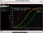
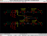
I want to use varactors to get the tuning curves but I am confused as to which varactor should be chosen among the available. Also, can the varactor type be identified by looking at the schematic? Attached is the figure for the reference. It's a NMOS varactor but is it a accumulation or an inversion MOS?

please also describe how to simulate this varactor to get Cg/Vg or Cg/Vtune curves?
please also describe how to simulate this varactor to get Cg/Vg or Cg/Vtune curves?


")