Continue to Site

Welcome to EDAboard.com

Welcome to our site! EDAboard.com is an international Electronics Discussion Forum focused on EDA software, circuits, schematics, books, theory, papers, asic, pld, 8051, DSP, Network, RF, Analog Design, PCB, Service Manuals... and a whole lot more! To participate you need to register. Registration is free. Click here to register now.

[Moved]: bizzare buffer AC response

Status
Not open for further replies.

mburakbaran

Member level 2
Joined
Jan 18, 2010
Messages
44
Helped
0
Reputation
0
Reaction score
0
Trophy points
1,286
Location
leuven
Activity points
1,724
Hello all,

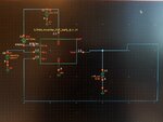
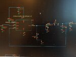
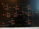
In one of my schematic level designs, for an analog amplifier, PM is supposedly 92 degrees. But when I used it in a buffer configuration, i noticed that for a square pulse, there were ringing during the slewing! I never experienced something like that. It could ring during settling and stuff, but during slewing??
There is possibly a zero in the system, it is causing the phase go up and down for a while when the freq increased, but it never causes PM to be problematic. The gain margin is also like 12dB or sth like that.

So, I connected the circuit again in buffer configuration (unity gain) and did an ac analysis. Normally you expect it to start from 0 dB, and after the GBW it should go down. But I noticed, my circuit, the gain first drops, and around 6-7 MHz it starts going up again, reaches upto 7dB, and then goes down again...

What are your thoughts?

Thanks in advance...
 

Re: bizzare buffer AC response

What are your thoughts?

I think you're right: There is probably a zero in the system, it is causing the gain go up.
around 6-7 MHz it starts going up
 

Re: bizzare buffer AC response

edaboard_gain_phase_open.pngedaboard_gain_phase_closed.png

Here are the open loop and closed loop AC simulation results.
Can we say that the PM seen at the open loop is just an illusion?
 

Please show the test circuit.

The closed loop magnitude plot doesn't fit the loop gain plot for unity (and any reasonable) feedback factor. There may be a feedforward path in your circuit, bypassing the amplifier.
 

It looks like you have a right half plane zero somewhere. In the open loop, you can see your phase dropping while your gain slope has been arrested due to the zero canceling the pole. Since you connected this in unity gain configuration, it's easier to see since slight changes in gain are more significant. If you've got miller compensation, you probably need to use a feedforward resistor, and if you have one, you need to size it properly.
 

Please show the test circuit.

The closed loop magnitude plot doesn't fit the loop gain plot for unity (and any reasonable) feedback factor. There may be a feedforward path in your circuit, bypassing the amplifier.

Thank you for the reply.

It's a conventional diff pair followed by a source follower (actually it's a flipped voltage follower but I do not think it has anything to do with this issue). Right at the output of the diff pair (or at the input if the source follower), there s an intentional parallel 10pF capacitance. I have used this to deliberately reduce the GBW it also does the stabilization work naturally, that node being the only high impedance one. To also have much gain and further reduce the GBW, the input transistors have quite some big areas. (I mean big as 200u width and 100u length, yes that is correct, that big...).

The closed loop is unity gain, I guess no need to say anything about it. The open loop is however is like this, at the output of the amplifier there s a VCVS with a gain of one, this is followed by a huge series L and a parallel huge C, which is followed by another VCVS with unity gain. This is connected to the negative input of the amplifier. This theoretical elements are used to closed the loop DC wise. To make things more realistic, I also tried connecting a dummy amplifier right before the first VCVS to also see the effect of the probable huge input capacitance during the closed loop operation. But I still do not see that awkard behaviour when it is closed loop just like the above graph. When it is unity gain however, it is problematic as can be seen at the other graph above... Still puzzled.

- - - Updated - - -

It looks like you have a right half plane zero somewhere. In the open loop, you can see your phase dropping while your gain slope has been arrested due to the zero canceling the pole. Since you connected this in unity gain configuration, it's easier to see since slight changes in gain are more significant. If you've got miller compensation, you probably need to use a feedforward resistor, and if you have one, you need to size it properly.

Hello. Thank you, please take a look at the response to FvM's post. The compensation is not miller, details are in there.
 

Your test circuit description doesn't seem to explain the irregular closed loop gain plot.

In case there could be a circuit flaw hidden in the verbose description, I would prefer to see a schematic.
 

Your test circuit description doesn't seem to explain the irregular closed loop gain plot.

In case there could be a circuit flaw hidden in the verbose description, I would prefer to see a schematic.

Hello again, here are the schematics for the circuit itself, and the higher hierarchy tests views. Rout you see at the output is 10k ohms (output is low impedance thanks to the source follower anyway).
 

Attachments

  • 23627333_1702032159861119_225109665_o.jpg
    23627333_1702032159861119_225109665_o.jpg
    207.9 KB · Views: 187
  • 23558221_1702032163194452_964524449_o.jpg
    23558221_1702032163194452_964524449_o.jpg
    233.8 KB · Views: 167
  • 23585375_1702032169861118_409513498_o.jpg
    23585375_1702032169861118_409513498_o.jpg
    238.5 KB · Views: 176

Thanks. I don't recognize how the gain peaking around 7 MHz takes place. To achieve this, the loop gain must rise near unity, which doesn't seem plausible looking at the open loop gain plot.

It looks like the open loop gain > 1 MHz is changed in the feedback configuration. The only obvious difference is that the Vin- node is connected in parallel with relative large rout. You could check if adding an ideal buffer between rout and Vin changes the closed loop gain.
 

Is there any particular reason why you have 1pF at the output of the second stage? Is that your load? If you're trying to compensate, you should do that at the output of the OTA stage, where you have the highest impedance. If you do it in the second stage as well, you're bringing in that pole closer to the dominant pole, which will worsen your stability. If that is a load capacitance, you might need to further decrease your output resistance so you can push that pole out further. Also, it may be possible that you might be seeing resonance as a result of interaction between two poles that are too close together. I have seen this behavior with source followers and flipped voltage followers that make use of local feedback.
 

Thanks. I don't recognize how the gain peaking around 7 MHz takes place. To achieve this, the loop gain must rise near unity, which doesn't seem plausible looking at the open loop gain plot.

It looks like the open loop gain > 1 MHz is changed in the feedback configuration. The only obvious difference is that the Vin- node is connected in parallel with relative large rout. You could check if adding an ideal buffer between rout and Vin changes the closed loop gain.

edaboard2.jpgEDABOARD.png

Hello again, I tried what you suggested, and it indeed corrects the behaviour as can be seen from the graphs. So, huge input capacitance and combination of Rout is causing this? If so, why do we still do not see this in the closed loop, when I also add a dummy replica of the circuit to the output of the original one, to mimic the huge output capacitance coming to the output node when the unity feedback connection is made? Wonders wonders.

- - - Updated - - -

Is there any particular reason why you have 1pF at the output of the second stage? Is that your load? If you're trying to compensate, you should do that at the output of the OTA stage, where you have the highest impedance. If you do it in the second stage as well, you're bringing in that pole closer to the dominant pole, which will worsen your stability. If that is a load capacitance, you might need to further decrease your output resistance so you can push that pole out further. Also, it may be possible that you might be seeing resonance as a result of interaction between two poles that are too close together. I have seen this behavior with source followers and flipped voltage followers that make use of local feedback.

Hi, that is just almost a random cap, say the cap that could come from the bondpad. I was also sweeping it from 1p to like 100p to see whether it is causing any abnormal thing for the phase margin, and it was not. Which is no suprise, since that node is a low impedance one... I hear what you are saying, however, what do you think about the discrepancy between open loop and closed loop simulations?
 

Status
Not open for further replies.

Similar threads

Part and Inventory Search

Welcome to EDABoard.com

Sponsor

Back
Top