Continue to Site

Welcome to EDAboard.com

Welcome to our site! EDAboard.com is an international Electronics Discussion Forum focused on EDA software, circuits, schematics, books, theory, papers, asic, pld, 8051, DSP, Network, RF, Analog Design, PCB, Service Manuals... and a whole lot more! To participate you need to register. Registration is free. Click here to register now.

[SOLVED] Sub-threshold Slope Factor

Status
Not open for further replies.

ANALA

Member level 1
Joined
Aug 7, 2017
Messages
33
Helped
0
Reputation
0
Reaction score
0
Trophy points
6
Activity points
264
Sub-threshold slope factor is given by :
[1+ Cd/Cox]
Cd = depletion capacitance
Cox= oxide capacitance

How to calculate the Sub-threshold slope factor for different technology nodes? I m able to substitute for Cox but i don't know how to calculate Cd...i m using the basic inverter circuit
 

How to calculate the Sub-threshold slope factor for different technology nodes?

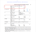
The sub-threshold (or: weak/moderate inversion) slope factor n0 doesn't change a lot with process size, see e.g. this snippet from Binkley's book:
Binkley__Tradeoffs_and_Optimization_in_Analog_CMOS_Design_p43.png
 

Not familiar with the "n0 slope factor" but in my experience
the subthreshold slope as mV/decade (log Id vs Vgs) is
very variable across process generations. The surface
states density (NSS) is key (along with the gate's authority
over those surface states). Surface state density has
to be discovered, not predicted - there's no good analytical
model for dirt and too-fast oxide growth.

Feature size is a "sorta" proxy for Tox and gate authority.
The tables that show n0 over a range of process L, stop
way short of (1) history and (2) higher voltage present-
day technologies.
 

I m using 32nm V2.0 Bulk CMOS PTM model file...
vt= 26e-003; %thermal voltage%

eo= 8.854e-14; %permittivity of free space%
er= 3.9; % relative permittivity of Silicon dioxide%
toxe= 7.5e-010; %electrical oxide thickness%
eox= eo*er; %permittivity of Silicon dioxide%
cox= eox/toxe; %oxide capacitance%

esir= 11.68; % relative permittivity of Silicon%
esi= esir*eo; %permittivity of Silicon%
nch= 4.1e+018 ; %channel concentration%
ni= 1.45e+010; %intrinsic concentration%
q= 1.602e-019; %electron charge%

num= 4*esi*vt*log(nch/ni);
deno= nch*(q);
xdep= (sqrt(num/deno)); % Maximum depletion width%
cdep= esi/xdep; %depletion layer capacitance%
m= 1+(cdep/cox) %subthreshold slope factor%

I was unable to find the value of channel doping concentration in the PTM model file...So i have assumed the value (roughly extracted from the graph)..using the above mentioned mentioned values, Sub threshold slope factor is approximately around 1.But i have read few articles where they have mentioned that for bulk CMOS m is around 1.4...May i know which value has to be used for the simulation and how do i justify that?
GRAPH.JPG
I have attached the graph from which i have roughly extracted the Nch value...
Link for PTM model file has been attached :http://ptm.asu.edu/latest.htmland i m using 32nm PTM model for metal gate/high-k CMOS: V2.0
 

... mentioned that for bulk CMOS m is around 1.4...May i know which value has to be used for the simulation and how do i justify that?

You could extract the subthreshold slope factor from of a simulation plot of log(Ids) vs. Vgs in subthreshold range. From the slope S of this curve you can extract the subthreshold slope factor
(here called n, respectively n0):

From David M. Binkley's book "Tradeoffs and Optimization in Analog CMOS Design" , p.14 :
Often the MOS weak inversion slope factor is expressed by the weak inversion or subthreshold swing given by
S=ln(10)nUT =2.303·nUT (mV/decade) (2.7)
This is the required increase in gate–source voltage for a factor-of-10 increase in drain current. The weak inversion swing is approximately 90 mV/decade for bulk CMOS processes at room temperature, assuming n = 1.5 and UT = 25.9 mV.

Find here a snippet from this book about the subthreshold slope factor: View attachment Binkley__substrate-factor.pdf
 
  • Like
Reactions: ANALA

    ANALA

    Points: 2
    Helpful Answer Positive Rating
I m using 32nm V2.0 Bulk CMOS PTM model file...

...
nch= 4.1e+018 ; %channel concentration%
...

In the ASU model files linked, I see:

+ngate = 1e+023 ndep = 4.12e+018 nsd = 2e+020 phin = 0

Where ndep looks like a sane VT-implanted value to me
(especially given its proximity to an equally sane and
obvious source/drain doping param).
 

Status
Not open for further replies.

Part and Inventory Search

Welcome to EDABoard.com

Sponsor

Back
Top