Continue to Site

Welcome to EDAboard.com

Welcome to our site! EDAboard.com is an international Electronics Discussion Forum focused on EDA software, circuits, schematics, books, theory, papers, asic, pld, 8051, DSP, Network, RF, Analog Design, PCB, Service Manuals... and a whole lot more! To participate you need to register. Registration is free. Click here to register now.

Line Driver circuit DC offset

Status
Not open for further replies.

Saltwater

Member level 3
Joined
Aug 30, 2015
Messages
64
Helped
0
Reputation
0
Reaction score
0
Trophy points
1,286
Activity points
1,867
Hi,

I have these SN75176 line drivers. And I was trying to see if I could hack some skew to the DC offset.
One circuit working on a testbench was the following circuit.
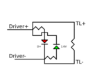
UnbalancedDriver.png

I have some questions tho.. Is this circuit any good for stability, "adding resistance and impedance down the line"?
Given it's just making square waves.


Regards,
 
Last edited:

"hack some skew to the DC offset"? What does that mean? Your whole question doesn't make a lot of sense.
 

Hi,

I want to adjust the DC offset of the line driver. It's a +DC -DC line driver and I want to try and get both voltages from 1% to 0.1% matched. "Or more".
I'm trying to use the chip's driver capabilities, and put a circuit on the end to get the result of being able to hand match the driven lines.

- - - Updated - - -

I wanted to add the link.

SN75176

- - - Updated - - -

Also Here's an updated schematic.
CircwietAuphgeraumdt.png
 

Hi,

The DC offset of such a driver is not important.
Indeed it can be anywhere between GND and VCC.

So what's the idea behind it?

In my eyes it makes no sense.

Klaus
 

So I have a ~±1% line driver. I want to use trimmers and trim it so that the voltages respectively are just right. Then I want to vary the load to get a voltage.
And logic toggle it using FPGA, To see how well it's going to perform in the Hz to MHz range.
Also I'm trying to isolate the circuit from ground. on a board this just seemed to work.
But i'm fuzzy on the electrical implications of doing any of this.
 
Last edited:

Hi,

Again: what is this good for?

Klaus
 

I'm sorry, but in all my years on this board I have never seen such an addled, incomprehensible post. "trim it so the voltage "respectively" is just right". That doesn't mean anything.

Perhaps this is a language/translation problem; if so, I'm sorry but I just don't understand. But this is going nowhere.

Good luck.
 

Hi,

Again: what is this good for?

Klaus

Getting an audible square wave.

I'm wondering would the timing of the diodes affect the circuit all that much. It would spike right?
I was trying to find a resistor method of doing this.

- - - Updated - - -

Matched? Matched to what?

Matched positive and negative rail of a ± line driver IC. "Srry, it's a logic to line driver IC"
 
Last edited:

Hi,

And why do you use a digital logic circuit for this?
Why not an analog switch, or a low power H bridge, or a class D amplifer?

Klaus
 

Analog is slow, H bridge is expensive, and complex. And I have like 100s of these drivers.
Would the schematic be any good?
 

I'm just as confused.
You mention Hz to MHz range then say it is for audio.
What are the red and green LEDs for?
It would help if you showed your proposed schematic with the 75176 as part of the diagram instead of using ambiguous names for the signals.

Brian.
 

The datasheet for the SN75176 shows on graphs fig1 and fig2 that the output high voltage loss is very different to the output low voltage loss and they cannot be matched like you want.

A squarewave sounds like a buzzer. The duty-cycle of the high time to the low time determines how much even harmonics are added to the odd harmonics of a squarewave. With audio frequencies and higher, both LEDs will light the same and will look like they are both turned on together. Changing the duty-cycle with Pulse Width Modulation (PWM) increases the brightness of one LED while it dims the other LED.
 

Hi,

Analog is slow, H bridge is expensive, and complex.
It seems you don't know what you are talking about.
* Analog switches are not slow
* and integrated H-bridges are neither expensive, nor complex.

And the DC offset of a differential driver has nothing to do - and doesn't harm "audible square wave".

Klaus
 

Adding a pullup resistor to one side and a pulldown to the
other (plus, minus) will give you a DC imbalance. Used to
do this to "crutch" the failsafe operation of line receivers
when customers insisted on interposing series resistors
between the line and input pins (degrading the open circuit
failsafe margin).

The common mode offset should be a don't-care. Differential
skew is going to make a bit of duty cycle distortion out the
back of the receiver (but if the transmission line and the
driver edges are crisp, not much effect until you get to near
minimum overdrive for functionality).

With a big enough junk box you can do anything. Doesn't
mean that doing a particular thing with junk at hand, is a
good or even practical idea.
 

Srry for the delay don't want to be snoody..

betwixt said:
What are the red and green LEDs for?
It would help if you showed your proposed schematic with the 75176 as part of the diagram instead of using ambiguous names for the signals.

Those are not leds, they are supposed to be "color coded" diodes to buffer the the resistance to a certain extent so I can self skew the circuit away from using a powered circuit.
The goal is to see if I can make a ladder DAC for my FPGA. Trimming these drivers. But unless it actually works right, it's not what I envision using.
However the 1.6V away from 1A is enough to balance the circuit. It's not providing the less than 1% tolerance when provided with the load resistance of the ladder DAC.

Audioguru said:
The datasheet for the SN75176 shows on graphs fig1 and fig2 that the output high voltage loss is very different to the output low voltage loss and they cannot be matched like you want.

A squarewave sounds like a buzzer. The duty-cycle of the high time to the low time determines how much even harmonics are added to the odd harmonics of a squarewave. With audio frequencies and higher, both LEDs will light the same and will look like they are both turned on together. Changing the duty-cycle with Pulse Width Modulation (PWM) increases the brightness of one LED while it dims the other LED.
I'm well aware of those effects (Audio designer, mathematician). Tho I did harm the integrity (symmetry under load) of my build by doing the diode thing.

Adding a pullup resistor to one side and a pulldown to the
other (plus, minus) will give you a DC imbalance. Used to
do this to "crutch" the failsafe operation of line receivers
when customers insisted on interposing series resistors
between the line and input pins (degrading the open circuit
failsafe margin).

The common mode offset should be a don't-care. Differential
skew is going to make a bit of duty cycle distortion out the
back of the receiver (but if the transmission line and the
driver edges are crisp, not much effect until you get to near
minimum overdrive for functionality).
The problem is when I do this, the leakage voltage between the added PSU + and - potentials is going to erase the driver being at 0.
So what i'm ultimately looking for is, and being able to tune both the ± drivers combined with performance under a varying load (buffered).
Or find ways to use different parts maybe, but I don't really consider these to be junk. Probably would waste a bunch of the expensive resistors even if I had to neglect the downphase of the DAC?
 
Last edited:

Hi,

The goal is to see if I can make a ladder DAC for my FPGA
I had a look at the datasheet. There are two charts for output characteristic HIGH and LOW.
For a fixed resistance you may have difficulties to be successful.
Mind "resistance". But you speak of "slow", therefore I assue you are interested in some speed. And then you usually don´t have (almost pure) resistance anymore but complex impedance.
I doubt that a fixed "compensation" can do the job.

with performance under a varying load
But for varying load I´d say it is impossible.

But I´m really curious what performance (resolution, DNL, INL) you expect and how close you get it running... with what range of load.

Keep us informed.

Klaus
 

I can do about 72Mhz on one of my good crystals, about 200Mhz using the pll. But it is audio band, so the ultrasound itself is not needed for this application. I think for my application I can have it lowpass filter itself out with no prob.

Pff, It's full of paradoxes right.. I took a look at my initial board driver levels, they are all spot on (outside a promile).

But for varying load I´d say it is impossible.
Yes, I think it's getting very hard.
 
Last edited:

Status
Not open for further replies.

Similar threads

Part and Inventory Search

Welcome to EDABoard.com

Sponsor

Back
Top