bio_man
Full Member level 2
Hi,
I want to convert my layout to GDSII required by MOSIS. I am using Cadence Virtuoso and I get the gds file by doing :
from CIW:
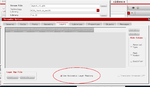
File >> Export >> Stream
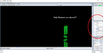
The gds file I got is only 50kB of size! is that usually the case, i feel this is not too much? my layout is 4mm2 and I have over 500 transistors and some big capacitors.
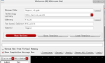
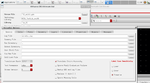
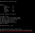
The second question, I want to see the GDS graphically and/or 3D. I found this software (https://www.youtube.com/watch?v=F4EArOqNNSU) but it requires a Process Definition file, I tried to make one by translating the technology (C5 technology) layer map into their way of writing the file but did not work, I always got an error that there is no substrate layer? although I added it into the txt file.
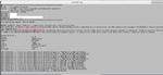
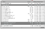
I attach both the Process layer map from MOSIS and GDS3D software process definition file and their readme file. I hope one can suggest what I need to do to make this readable to GDS3D software.
I want to convert my layout to GDSII required by MOSIS. I am using Cadence Virtuoso and I get the gds file by doing :
from CIW:
File >> Export >> Stream
The gds file I got is only 50kB of size! is that usually the case, i feel this is not too much? my layout is 4mm2 and I have over 500 transistors and some big capacitors.
The second question, I want to see the GDS graphically and/or 3D. I found this software (https://www.youtube.com/watch?v=F4EArOqNNSU) but it requires a Process Definition file, I tried to make one by translating the technology (C5 technology) layer map into their way of writing the file but did not work, I always got an error that there is no substrate layer? although I added it into the txt file.
I attach both the Process layer map from MOSIS and GDS3D software process definition file and their readme file. I hope one can suggest what I need to do to make this readable to GDS3D software.
Attachments
Last edited: