Continue to Site

Welcome to EDAboard.com

Welcome to our site! EDAboard.com is an international Electronics Discussion Forum focused on EDA software, circuits, schematics, books, theory, papers, asic, pld, 8051, DSP, Network, RF, Analog Design, PCB, Service Manuals... and a whole lot more! To participate you need to register. Registration is free. Click here to register now.

[Moved]: Modified PMOS Load Circuitry

Status
Not open for further replies.

promach

Advanced Member level 4
Joined
Feb 22, 2016
Messages
1,199
Helped
2
Reputation
4
Reaction score
5
Trophy points
1,318
Activity points
11,636
I have few questions regarding the modified PMOS load circuitry for Figure 15.18(c)

1) Why does M3 and M4 consume only a voltage headroom equal to |VDS3,4| after the addition of NMOS source follower ?

2) When M3 operates at the edge of the triode region, why is small-signal resistance of the load roughly equal to 1/gm3 ? I suppose it should be 1/gm5 ?

3) Could anyone elaborate on "the finite output resistance of the follower may yield an inductive behavior for the load" ?

Screenshot retrieved from Razavi Design of Analog CMOS Integrated Circuits 2nd Edition book.
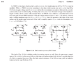
Screenshot from 2017-11-07 19-29-28.png
 

Re: Modified PMOS Load Circuitry

Quick Edit:
replace question 2 with the following :

2) Why "the time constant is smaller than that of a diode-connected transistor" ?
 

1 - Razavi is trying to illustrate that instead of a headroom requirement of Vgs the headroom consumed by the M3 and M4 device is just Vds which is less than the Vgs since the Vgs of the M5/M6 device is subtracted from it to set the Vds
2 - The time constant is smaller than the diode-connected transistor since the small signal resistance is still the same as 1/gn3 but now the capacitance is effectively reduced since the Gate to source capacitance of M3 or M5 does not have to be driven by the node X but is driven by the source follower.
3 - If we include the Cgs capacitance of M3 in the small signal equations we see that if gm5 due to its finite value at some frequency will not be able to drive the Cgs3 effectively making the drain of M3 look more and more like a current source thus the impedance will increase with frequency and that is the inductive behavior.
 

if gm5 due to its finite value at some frequency will not be able to drive the Cgs3 effectively making the drain of M3 look more and more like a current source thus the impedance will increase with frequency and that is the inductive behavior.

It makes me think that gm is actually dependent on frequency. Please correct me if I am wrong in this case.
 

gm is not dependent on the frequency but the Cgs impedance is. As the frequency increases the impedance decreases requiring more drive.
 

As the frequency increases the impedance of Cgs decreases requiring more drive.

How is this inductive ? How is drain of M3 becoming more and more like a current source ?
 

Inductive in terms of its impedance behavior. When the impedance seen at a point increases with frequency that is similar to an impedance shown by an inductor.
If the gate of M3 becomes a small signal short or if the magnitude of small signal diminishes on the gate then that means the gate is biased with a constant voltage irrespective of the signal in the other parts of the circuit. When a MOS is biased with a constant voltage it just becomes a DC current source with a high impedance.
 
Status
Not open for further replies.

Similar threads

Part and Inventory Search

Welcome to EDABoard.com

Sponsor

Back
Top