Continue to Site

Welcome to EDAboard.com

Welcome to our site! EDAboard.com is an international Electronics Discussion Forum focused on EDA software, circuits, schematics, books, theory, papers, asic, pld, 8051, DSP, Network, RF, Analog Design, PCB, Service Manuals... and a whole lot more! To participate you need to register. Registration is free. Click here to register now.

Help! 9V-32V step down to 5V switching regulator?

Status
Not open for further replies.

maviszeref

Newbie level 4
Joined
Oct 31, 2017
Messages
5
Helped
0
Reputation
0
Reaction score
0
Trophy points
1
Activity points
46
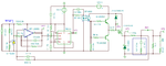
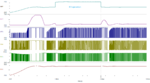
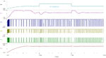
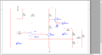
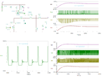
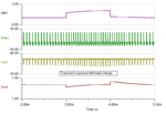
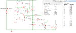
Hi. My professor wants us to design a switching regulator with an input of 9V to 32V, which will be regulated to 5V. Our circuit design is shown below. I thought that the design is a switching regulator since it has a switching waveform and an efficiency of 81 to 87% according to my simulation. I don't quite understand what he meant that it is not a switching regulator instead a linear regulator since there's no feedback. I thought lm393 provides the feedback.:thinker:
Please help me understand how can we say that it is switching or linear regulator. Thanks
 

Attachments

  • Screenshot (101).png
    Screenshot (101).png
    33.3 KB · Views: 138

Hi,

The problem with your circuit is, that it switches ON/OFF somehow by accident.
There is no forced frequency with a clean duty cycle control.
You may try to convince your professor by telling him it is a self resonant circuit.
(Don't expect much positve feedback)

I assume he wants to see:
* a freqency generator (maybe with sawtooth waveform)
* an error amplifier
* a comparator that compares both signals an thus generates the PWM.

Tell him how you calculated frequency, and duty cycle vs output voltage...and how you ensured output voltage stability.

Klaus
 
Thank you KlausST, I will try to make a new design. By the way, where do I measure the frequency, is it under the gate of the PMOS? just for comparison of the measured and calculated.
 

A self-excited hysteretic buck converter. Not fixed
frequency PWM, but was that asserted as a requirement?

If you can show that it switches, and regulates, then
there you are. Does it?
 

If you have designed it yourself, it is certainly very interesting.

I do not understand how it works (and if it works at all) but since you have done it it deserves a credit.

L1 is the key component; it allows the voltage to ramp up slowly enough so that the series pass may be effective. But perhaps you will have lots of noise.
 

Hi,

Thank you KlausST, I will try to make a new design. By the way, where do I measure the frequency, is it under the gate of the PMOS? just for comparison of the measured and calculated.

Because of this question I doubt that you designed the circuit on your own. You should know the path with switching signals (frequency).

Klaus
 

Honestly, the circuit is made through several researches on internet and we've just made some modifications. We lack knowledge about this stuffs, do you have any references where we can deeply understand switching regulator? Thanks
 

I agree with dick_freebird, you should hold the circuit against the given exercise problem specification. If there are no conflicting requirements, your circuit can be considered a valid solution (after necessary corrections, see below).

I don't quite understand what he meant that it is not a switching regulator instead a linear regulator since there's no feedback.
I neither do because the analysis is incorrect in two respects, related to the present circuit and as general statement. Either you got the comment wrong or your professor doesn't understand the self-excited hysteretic circuit operation.

The schematic has however errors and won't work as shown. I presume R12 is intended to connect to U2A.1 while U2A.8 should connect directly to 9V supply. LM393 output is open collector and can't drive a load without pull-up current. R8 is causing unwanted slow MOSFET turn-on and respective switching losses. It should be either removed or have a considerably lower resistance.

Most switch mode converters have a dedicated oscillator and pwm modulator, you can review classical pwm controller datasheets like SG3524.
 
The problem with these simple hysteresis types switching regulators is to get the switching frequency high enough with sufficient ripple filtering of the output voltage. Ideally, you want it at least around 20 KHz, but if you pick decent LC combinations, it forces the switching frequency down. Another problem is that the switching frequency is also load dependent.

One way I found to help keep the frequency high enough is to employ a two-stage LC filter.
The first-stage values are small enough to enable good switching frequency, while the second stage provides the required extra filtering. The second stage is kept out of the feedback loop for stability reasons.

The modified diagram below is an example of implementing this idea. These regulators can be very efficient, due to the fast switching speed of the PMOS device, as can be seen in the simulation. In some of my experiments, I have achieved efficiencies touching 95% employing low loss power parts. They work well with a constant load, but can be a problem with widely varying loads or very light loads.

I have commented about these regulators in other treads:
https://www.edaboard.com/showthread.php?t=362915
https://www.edaboard.com/showthread.php?t=331961

Here is the web address of the person who claims to be the creator of the original idea.
https://www.romanblack.com/smps/smps.htm
 

Attachments

  • step_dn.png
    step_dn.png
    94.4 KB · Views: 121
  • load_ch.png
    load_ch.png
    20.1 KB · Views: 109
Here is a design I did some time ago for regulating down to 12 V from 48 V. The simulator predicted 97% efficiency, but I could only measure 95% at 1 A output. I think I had a bit more loss in my inductor. Switching frequency is about 19 kHz.

Included is a breakdown of dissipation for the various components.
 

Attachments

  • 48_12.png
    48_12.png
    56.6 KB · Views: 135

Thank you for the references E-design. I think my professor wanted to see a frequency generator, an error amplifier
and a comparator that compares both signals which generates the PWM, just like what KlausST said. This is our new circuit design, do you have any comment or suggestion for this circuit? Thanks Screenshot (104).png
 

Many circuit details need correction. I presume you'll it see when simulating the circuit.

- triangle generator component values, R5/R6 for reasonable hysteresis, consider limited LM741 common mode range, correct C2 R4
- LM393 pull-up resistors, remove R12
- reasonable gate driver, consider gate voltage absolute maximum rating
- use a PI error amplifier in place of comparator U2A
 
Thank you for FvM, can you give me an example of a PI error amplifier and a gate driver?
 

@e-design: Post #10 shows D1 and D9 in parallel with no series resistor (negative feedback). How did you managed both of them to be matched ?

give me an example of a PI error amplifier
Page 8,fig5.
 

If you are interested in hysteretic controllers, Texas Instuments has on its website a few videos and presentations explaining them:

https://training.ti.com/buck-regula...teretic control&tisearch=Search-EN-Everything

Like all semiconductor companies, after a brief introduction they will immediately switch to promote their products.
Nevertheless it provides a good overview and discusses pros and cons of this architecture.
 

@e-design: Post #10 shows D1 and D9 in parallel with no series resistor (negative feedback). How did you managed both of them to be matched ?

In my practical circuit, I ended up using a single SiC diode. Interestingly the efficiency only dropped 1% going from 1 A to 2A output current. I got better low loss chokes from Coilcraft since then, so I would like to revisit the circuit sometime.
 
  • Like
Reactions: CataM

    CataM

    Points: 2
    Helpful Answer Positive Rating
One can also use the trusty old 555 and manipulate it to serve as a pulse controller as shown below.

With the chips available today, this is hardly a practical design but can be valuable information to some students and hobbyists.

It manages to operate between 9-32 V of input voltage, but struggles a bit at 9 V, with the error amp almost bottomed out. I have the chip running of an 8 V supply which could be obtained from a low drop-out regulator capable of supplying about 40 mA and handle the 32 V input as well.

Load-transient response isn't too shabby and behaves reasonably well over the full input range and providing a 5 V output. The error op-amp must be able to swing near the rails. The ripple can be further cleaned up with another LC filter if needed.

This is just a design idea, not tested on the bench!
 

Attachments

  • 555_1.png
    555_1.png
    50.9 KB · Views: 118
  • 555_2.png
    555_2.png
    123.5 KB · Views: 108
  • 555_3.png
    555_3.png
    77.6 KB · Views: 107
Status
Not open for further replies.

Similar threads

Part and Inventory Search

Welcome to EDABoard.com

Sponsor

Back
Top