Continue to Site

Welcome to EDAboard.com

Welcome to our site! EDAboard.com is an international Electronics Discussion Forum focused on EDA software, circuits, schematics, books, theory, papers, asic, pld, 8051, DSP, Network, RF, Analog Design, PCB, Service Manuals... and a whole lot more! To participate you need to register. Registration is free. Click here to register now.

Sequential Circuit Timing Analysis

Status
Not open for further replies.

farabi2017

Newbie level 3
Joined
Nov 2, 2017
Messages
3
Helped
0
Reputation
0
Reaction score
0
Trophy points
1
Activity points
51
For the circuit shown below, the timing parameters of its components are: tAND = 0.4ns, tbuf = 0.2ns, tsetup = 0.2ns, thold = 0.2ns, and tclk→Q = 0.4ns. When answering the following questions, you need identify the path used in your computation.
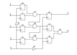
06.JPG

1.1) Calculate its maximum clock frequency.
1.2) Calculate its clock to output delay.
1.3) Calculate its external setup time.
1.4) Calculate its external hold time.
1.5) Show how you can improve the circuit clock frequency to 2.5GHz. Note that the modified circuit should keep the same function and cannot have other timing violations.
 

Hi,

I´d use a colored pen and mark the paths for the different cases with different colors. Then write the timings across the marked components. And then find out the timing that relates to the questions (mainly by adding / subtracting the time values).

begin with the paths for 1.1.

Klaus
 

Hi,

Okay, that'd be fine. Can you please help me identifying the different paths for different cases?
 

Hi,

Okay.
You know what the clock signal is? It has a source and it has some targets (= components).
And there are connections (data) between one clocked component and another clocked components.

Mark them and show us your result.

Klaus
 

The circuit is not complete, the clock input on U1 isn't even connected to anything. I'm assuming you meant to connect it to the output of U13 (or not).

Here is an hint:
The longest path between registers is U12-U7-U8-U10-U9
 

1) The max. freq. would be 1/1.8ns = 555.55MHz
5) To make the circuit work at 2.5 GHz (0.4 ns)
5.1) Delay the clocks for output flops, so that skew will be more.
-- for first output flop add 3 more buffers (0.6 ns)
-- for 2nd output flop add 5 more buffers ( 1 ns)
-- for 3rd output flop add 7 more buffers (1.4 ns)
5.2) Delaying the clocks will violate hold requirement. So delay the data paths by adding buffers after the outputs of first stage flops
-- Add 3 buffers (0.6 ns) after the output of 3rd flop of first stage (for which input is c)
-- Add 5 buffers (1 ns) after the output of 4th flop of first stage (for which input is d)


Regards,
Ashish
 

2) clock to output delay
e to o1 : 0.2 + 0.4 = 0.6 ns
e to o2 : 0.2 + 0.4 + 0.4 = 1 ns

3) external setup time <= min clock period - max clock to output delay
<= 1.8 - 1
<= 0.8 ns

4) external hold time <= min clock to output delay
<= 0.6 ns
 

You can add more gates and make the critical path shorter. You need to AND a-b-c-d, which can be done in 2 stages instead of 3.
 

Status
Not open for further replies.

Similar threads

Part and Inventory Search

Welcome to EDABoard.com

Sponsor

Back
Top