Continue to Site

Welcome to EDAboard.com

Welcome to our site! EDAboard.com is an international Electronics Discussion Forum focused on EDA software, circuits, schematics, books, theory, papers, asic, pld, 8051, DSP, Network, RF, Analog Design, PCB, Service Manuals... and a whole lot more! To participate you need to register. Registration is free. Click here to register now.

I'm looking Full H bridge driver

Status
Not open for further replies.

carpenter

Full Member level 6
Joined
Jul 25, 2012
Messages
353
Helped
22
Reputation
44
Reaction score
24
Trophy points
1,298
Activity points
4,467
I need realise high current Full H bridge and search driver for Mosfet in bridge

- Voltage 80V
- MOSFET in driver 8x IPT012N08N5 2pcs parelel on every position
this MOSFET is 80V 300A Rdson 1,0mOhm , Input capacitance 13nF (26nF on two pcs)
drive signal ideal 3.3V logic from MCU

What I need from the bridge
1. Swing output with frequency 1-1000Hz and adjustable "duty cycle"
2. Set low side On and mege any PWM sequence on hifg side switch
3. Realise one shot from 1,s to 1s

Which controller would you recommend?

I find hip4081a, but not ideal and do not know how to charge 26nF., not 3.3V compatible
 

You're going to need more than 3.3V to drive those MOSFETS. The HIP4081 will accept 3.3V logic level inputs, even though it needs a higher supply voltage. I don't know of any driver that will run off only 3.3V that can drive those hefty MOSFETs.
 

I need realise high current Full H bridge and search driver for Mosfet in bridge

- Voltage 80V
- MOSFET in driver 8x IPT012N08N5 2pcs parelel on every position
this MOSFET is 80V 300A Rdson 1,0mOhm , Input capacitance 13nF (26nF on two pcs)
drive signal ideal 3.3V logic from MCU
I hope you don't intend to actually use an 80V supply for the H bridge. The FET Vds rating should be higher by at least 25%.
 

Thanks for the answers.
For clarification.
1. Transistors are at max voltage of 80V, but the voltage on devices does not exceed 60V. (80V is inclusive safe reserve)
2. 3.3V I think Logic level for signal not the supply voltage for driver. As power supply for driver have +12V pro driver and low side MOSFET , high side mosfet PS must be in bridge drivers.
In datasheet HIP4081A is "Input Logic Thresholds Compatible with 5V to 15V Logic Level" and in specification is for high temperature range Low Level<=0.8V and High Level>=2.7V STM32 on 3.3V have High Level on Five-volt tolerant IO >=1.55V, LVTTL 3.3V logic have High Level >=2.4V probably it will work, but .....
 

Hi,

The logic levels shouldn't be the problem. Just use a HCT buffer in front of the HIPxxx.

Klaus
 

A couple of queries.

1 Switching time and Delay resistor.
if I use two Infineon-IPT012N08N5 paralel on at each position , Driver must charge 2x 160nC, hip4081a have charge 2,5A
switching time =1,5*(Qg/I)= 216ns.
for delay resistor 200k Ohm is deadtime 100ms and 200k is max recomended resisotr.
it means that it does not have to use automatic timing?

2 Bootstrap diode?
As bootstrap diode I can use High-Speed Switching Diode MMBD914L 100V 200mA 4ns .
it's a good choice for switchimg frequency 1kHz?
 

delay resistor 200k Ohm is deadtime 100ns and 200k is max recomended resistor
 

I'll add a schematic
HB.png
 

Hi,

Use fast 1uF capacitors at 12V close to D3, D14..
Use an additional 100uF bulk capacitor at 12V

Why are your C4, C6 rated for 100V? They see only 12V, therefore a 16V or 20V rating should be OK.

Use bulk capacitor at VCC
Use fast capacitors at VCC close to the high side MOSFETs
Instead of D10, D11 use fast diodes to VCC and GND

What´s the use of D4, D6, D7....?

Why don´t you use the ALS and BLS feature?

Use a proper PCB layout with a rock solid GND plane.

Klaus
 

> Use fast 1uF capacitors at 12V close to D3, D14..
> Use an additional 100uF bulk capacitor at 12V
OK I add

> Why are your C4, C6 rated for 100V? They see only 12V, therefore a 16V or 20V rating should be OK.
I thing , If Vcc is max 60V will be gate chrarge voltage for high side MOSFET about 70V. If high MOSFET is ON and load is disconected is on C4 C6 more precise on AHS and BHS full VCC voltage therefore it should be bootstrap diode and capacitor dimensioned on min. VCC,but maybe I'm wrong with the capacitor voltage rating.


>Use bulk capacitor at VCC
yes, they are part of the Vcc source

Use fast capacitors at VCC close to the high side MOSFETs
I add 10uF 100V 1210 ceramic capacitor to every one high side MOSFET.


> Instead of D10, D11 use fast diodes to VCC and GND
I will think about it
> What´s the use of D4, D6, D7....?
Transient-voltage-suppression diode 15V for protection of Gate MOSFET, maybe they are useless

Why don´t you use the ALS and BLS feature?
What do you mean by the term "ALS and BLS feature"?


>Use a proper PCB layout with a rock solid GND plane.
Of course , I plan use 106um, base copper Weight and add several soldered copper wire on this base copper


When we talk about diodes
is a good idea replace two pcs MMBD914LT1 4ns fast diode in gate MOSFEET with Dual diode, common cathode
for example
BAT54C 30V Schottky Surge forward current tp < 1s 600 mA
BAS40-05 40V Schottky Surge forward current tp < 1s 600 mA
PMEG4005CT 40V Schottky IFRM repetitive peak forward 3.9A
all in SOT-23, switching frequency max 1000Hz
 

Hi,

I thing , If Vcc is max 60V will be gate chrarge voltage for high side MOSFET about 70V. If high MOSFET is ON and load is disconected is on C4 C6 more precise on AHS and BHS full VCC voltage therefore it should be bootstrap diode and capacitor dimensioned on min. VCC,but maybe I'm wrong with the capacitor voltage rating.
Imagine. Your cellular phone battery is 7.2V. You take your phone while you walk on a carpet...due to electrostatic effects you become charged with 10.000V. Now does your cellular phone battery need to be rated with 10.000V? No, there's still only 7.2V.
The same situation is with your bootstrap capacitor..

yes, they are part of the Vcc source
You need them on your PCB.

Transient-voltage-suppression diode 15V for protection of Gate MOSFET, maybe they are useless
The voltage limitation should be done by the HIPxxx device.

What do you mean by the term "ALS and BLS feature"?
Read the HIPxxx datasheet.

replace two pcs MMBD914LT1 4ns fast diode in gate MOSFEET with Dual diode,
I don't see what they are good for.

Klaus
 

> Why are your C4, C6 rated for 100V? They see only 12V, therefore a 16V or 20V rating should be OK.
I do not want to argue because in the case of a capacitor I'm really not sure
To your example
you are right, but you have a 10.000V protection at all intakes on your phone.
Back to bootstrap in **broken link removed**15 section Bootstrap diode is expressly recommended use diode with same or high blocking voltage as have shitching transistor.

>You need them on your PCB.
Yes will be one PCB , I draw it in Altium, many section and sheet, but one project and one PCB.

>The voltage limitation should be done by the HIPxxx device.
I was thinking of an crash, but you are right, they are useless

>What do you mean by the term "ALS and BLS feature"?
I read the datasheet, I admit I find it somewhat unclear, but ALS and BLS is only A and B Low-side Source connection. Connect to source of A and B Low-side power MOSFET.

>replace two pcs MMBD914LT1 4ns fast diode in gate MOSFEET with Dual diode,
I'll take it a little too wide
If MOSFET is Turn On , charge driver Gate over resistor (in my schematics 5.6Ohm) this resistor limits the current and prolongs the opening time, thereby improving EMC.
If MOSFET is Turn Off, driver discharge Gate over diode and shortens shutdown time.
In my case.
Driver on +12V have only max 2.5A charging current, i.e for driver charge 166nC over 100ns. 2pcs IPT012N08N5 have Gate charge total 360nC time of charge 216ns.
216ns is a relatively long time maybe the gate resistance is unnecessary
Diode clamp gate resistor and allows a higher discharge current.

Thank you for your help
 

Hi,

Bootstrap diode:
Yes it needs to be rated for the high voltage.

If you have a scope with differential voltage measurement, then you may lokk at capacitor voltage and diode voltage. Or use a simulation tool, or use a good bootstrap application note....like your given document..

ALS, BLS.
OK, I was not clear in this. With the use of these lines you can implement current control or overcurrent protection.
Often a useful feature...if the additional cost is not the problem.

If MOSFET is Turn Off, driver discharge Gate over diode and shortens shutdown time.
In my case.
True. This is the usual way when the driver doesn't have a dead time feature. But with the HIPxx you don't need this.
You say slowing down switch ON reduces EMI. This is true. But your fast switching OFF makes EMI worse.
If you want to reduce EMI you may control this with the series resistor...in both directions, without diode. And with the dead time feature you prevent the H bridge from cross conducting.

EMI.
The series resistor also prevents from high frequency ringing when switching ON a MOSFET. I recommend to use a series resistor.
The ringing is mainly influenced by the PCB layout and the stray inductances in your circuit. A bad layout may need higher ohmic resistors to prevent from ringing.

Don't be discouraged by my posts. You may and you should design your own circuit. And if you experience something strange with your circuit..then hopefully my posts help you to find an explanation.

Klaus
 

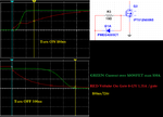
I tried simulating mosfets turning on and off 2pcs MOSFET IPT012N08N5 .

Datasheet hip4081a say Peak Pullup Current for 12V is 2.5A I simulate is as 12V/0V voltage source with 4Ohm resistor
Gate is Turned On over 10Ohm resisotr and Turned Off over 10Ohm resistor with diode PMEG4005CT

Turn On time is 180ns
Turn Off time is 500ns

Datasheet does not specify resistance or discharging current of resistence is 4Ohm too is TurnOff time 500ns.
hip4081a have internal delay TurnON-Delay max 110ns for 250kOhm DEL resistor.
i.e if I use only 2line driver and delay line will be 110ns is high side MOSFET open before the low side MOSFET is closed.

Gate.png
 

Status
Not open for further replies.

Part and Inventory Search

Welcome to EDABoard.com

Sponsor

Back
Top