Continue to Site

Welcome to EDAboard.com

Welcome to our site! EDAboard.com is an international Electronics Discussion Forum focused on EDA software, circuits, schematics, books, theory, papers, asic, pld, 8051, DSP, Network, RF, Analog Design, PCB, Service Manuals... and a whole lot more! To participate you need to register. Registration is free. Click here to register now.

Circuit biasing problem

Status
Not open for further replies.

promach

Advanced Member level 4
Joined
Feb 22, 2016
Messages
1,199
Helped
2
Reputation
4
Reaction score
5
Trophy points
1,318
Activity points
11,636
How to bias this circuit correctly ?

Gm2.png
 

How to bias this circuit correctly ?

Where? M5 has its bias voltage already. What's your Vdd ? Do you want it operate in open or closed loop? Which gain is required?
 

Vdd = 3.3V and closed loop operation. Large-signal gain or small-signal gain ? I guess I need to read some books to get the relevant gain equations.

Additional Information:

This diferential circuit is connected in negative feedback manner to a CMOS inverter.


frequency_trap.png

This is the overall schematics.
 

What do you intend with this circuit? If the X1 circuit actually is a digital inverter cell, it won't operate in linear mode. It could perhaps transform your sinusoidal input into a square wave output.
 

As far as I know, X1 is not a pure digital inverter cell.

CMOS_inverter_X1.png

- - - Updated - - -

As mentioned in https://www.edaboard.com/showthread.php?t=348802&p=1489127&viewfull=1#post1489127, could you elaborate on it ? inductor for open-loop gain measurement ? and how is CMFB circuit used in this case ?

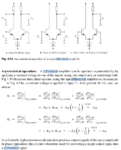
Besides, it seems like I have a similar differential amplifier as in Figure 4.54(a) below:

Why does the first term of A1 ends up as Ad while the second term ends up as Acm ?

Screenshot from 2017-10-12 17-59-53.png
 

As far as I know, X1 is not a pure digital inverter cell. View attachment 141769
As long as there's no feedback around it, it's considered pure digital.

As mentioned in https://www.edaboard.com/showthread.php?t=348802&p=1489127&viewfull=1#post1489127, could you elaborate on it ? inductor for open-loop gain measurement ?
I think it's well explained; a standard method for open-loop gain measurement. Reread it thoroughly, and read about it in any Analog Circuit Design textbook.
If you need more explanation, you should exactly tell about what.

and how is CMFB circuit used in this case ?
By control of the head or tail transistors.

Besides, it seems like I have a similar differential amplifier as in Figure 4.54(a) below:
Why does the first term of A1 ends up as Ad while the second term ends up as Acm ?
These are the definitions of the differential and common mode gain (or rather: transimpedance).
 

ok, let me read more on application of CFMB circuitry.

Is the following test circuit the right way to measure open-loop gain of my Gm2 circuit block ? note: now I have asymmetrical input rather than symmtrical differential pair

Screenshot from 2017-10-12 20-04-41.png
 

Yes, it's fine - if your amplifier is able to sustain an output common mode voltage OCMV=V2. A correctly dimensioned amplifier with feedback controlled gain |A|=1 (via L1 in your above circuit) will do it.
 

For a DC feedback gain of -1 , the amp output must be able to achieve an OCMV same as the DC non-inverting input voltage. So simple!
 

Status
Not open for further replies.

Similar threads

Part and Inventory Search

Welcome to EDABoard.com

Sponsor

Back
Top