Continue to Site

Welcome to EDAboard.com

Welcome to our site! EDAboard.com is an international Electronics Discussion Forum focused on EDA software, circuits, schematics, books, theory, papers, asic, pld, 8051, DSP, Network, RF, Analog Design, PCB, Service Manuals... and a whole lot more! To participate you need to register. Registration is free. Click here to register now.

How to understand this pulse load generation circuit

Status
Not open for further replies.

bhl777

Full Member level 6
Joined
Sep 30, 2008
Messages
363
Helped
0
Reputation
0
Reaction score
0
Trophy points
1,296
Activity points
5,140
Hi All, I saw a pulse load generation circuit design from Internet. I can understand some of the basic concepts, but would someone help me a thourougful understanding?

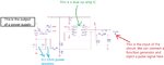
This is the schematic of this circuit. We can inject a pulse signal from the function generator, then the pulse signal will go to two op-amps to generate two drive signals OUTA and OUTB. They wil drive the powerFET to turn ON/OFF, and generate the pulse load current to go through power resistors.

load generator.jpg

I have some questions of this circuit:
(1) Why we need two signals to drive the power FET? How does OUTA and OUTB work individually?
(2) Why there is a 499 Ohm resistor (R45) connect to the two power resistors? What is it used for?
(3) Why there is a 22pF cap placed between the 2nd opamp's output and the inverting input? What is it used for?

Thank you!
 

Attachments

  • load generator.jpg
    load generator.jpg
    116.3 KB · Views: 66

1). I think that's just to increase the current drive of the mosfet gate capacitance.
2) this is providing feedback to control the load.
3) that cap is for noise reduction
 
  • Like
Reactions: bhl777

    bhl777

    Points: 2
    Helpful Answer Positive Rating
1). I think that's just to increase the current drive of the mosfet gate capacitance.
2) this is providing feedback to control the load.
3) that cap is for noise reduction

Thank you Barry! Would you advise me two additional questions?
(1) Regarding your answer #2, "this is providing feedback to control the load", would you advise how it works and why we need it? In another word, what will happen if we remove this 499 Ohm?
(2) What is the purpose of 3 Ohm resistor connecting to the gate? Can I say it is used with Cgs and some other parasitic caps inside the FET for some filtering purpose?

Thank you!
 

1) It's controlling current. As the voltage across RLT1/RLT2 rises it will drive the mosfet gate voltage lower.
2) It will minimize ringing.
 
  • Like
Reactions: bhl777

    bhl777

    Points: 2
    Helpful Answer Positive Rating
Combining OP outputs through 3 ohm resistors might work for some power OPs. If it's an arbitrary general purpose dual OP, I won't expect performance, possibly not even basic function.

But without knowing the exact OP type, it's just guessing.
 

Combining OP outputs through 3 ohm resistors might work for some power OPs. If it's an arbitrary general purpose dual OP, I won't expect performance, possibly not even basic function.

But without knowing the exact OP type, it's just guessing.


Hi FvM, thank you for your reminder. I will pay attention to the selection of the opamp. Would you also guess what are the purpose of R39,R41,R42 between the input pulse signal and the non-inverting input node INB+?
 

Those resistors provide a 50 ohm input impedance and a small attenuation.
 
  • Like
Reactions: bhl777

    bhl777

    Points: 2
    Helpful Answer Positive Rating
Status
Not open for further replies.

Similar threads

Part and Inventory Search

Welcome to EDABoard.com

Sponsor

Back
Top