Continue to Site

Welcome to EDAboard.com

Welcome to our site! EDAboard.com is an international Electronics Discussion Forum focused on EDA software, circuits, schematics, books, theory, papers, asic, pld, 8051, DSP, Network, RF, Analog Design, PCB, Service Manuals... and a whole lot more! To participate you need to register. Registration is free. Click here to register now.

Design of Single stage OTA with following specs

Status
Not open for further replies.

prateekj212

Newbie level 4
Joined
Apr 13, 2009
Messages
5
Helped
0
Reputation
0
Reaction score
0
Trophy points
1,281
Activity points
1,321
I am referring the design prcoedure from Philip Allens textbook from chapter 5.2.7. I am designing a single stage OTA with differential amplifier and current mirror load. My specifications are below:

DC Gain Av = 40 dB minimum
Gain-Badnwidth = 40MHz minimum
Large signal cut off frequency 200 kHz
Output common mode typical voltage 0.9 V
Input common mode range 0.3 to 1.4 V
Supply voltage VDD 1.8V
Load capacitance 1pF

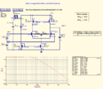
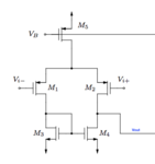
I am achieving the gain of 40 dB between 0.3 to 1.4V but my output common mode is stuck at 1.247 V which is not desired. I am using Cadence design tools. Here is the circuit below.

I am using NMOS differential pair.

Please help with proceeding with the implementation.

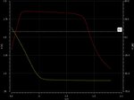
Screenshot (25).pngScreenshot (26).pngScreenshot (27).png
 

Output common mode typical voltage 0.9 V
... but my output common mode is stuck at 1.247 V which is not desired.

With this architecture, your output common mode voltage (OCMV) is determined by the W/L ratio of your PMOSFETs to that of your NMOSFETs: W/L(PMOSFETs) / W/L(NMOSFETs). For an OCMV≈0.9V you'll have to reduce this ratio probably far below 1 .

Find here an example for a (W/LPMOS)/(W/LNMOS) 1:20 ratio : 180nm-1stage-OTA-40MHz-1pf-OCMR-0,9V.png

Unfortunately, your ICMR will probably be restricted at the lower end.
 
  • Like
Reactions: e0e0

    e0e0

    Points: 2
    Helpful Answer Positive Rating
Hi
Thank you very much for the suggestion. I tried the simulation with the dimensioning mentioned by you. I achieve a output common mode value of around 900m but my gain suffers now. way less than 40 dB. I am not sure how you got 47 dB with your simulation. I am using the exact same dimenisions for the circuit PMOS and NMOS. Do i Need to increase the current beyond 10u?

Appreciate your help.

ICMR2.jpg
 

... but my gain suffers now. way less than 40 dB. I am not sure how you got 47 dB with your simulation. I am using the exact same dimenisions for the circuit PMOS and NMOS.
Different process? In any case different models!

Do i Need to increase the current beyond 10u?
No, quite the contrary - if you have enough UGB. See the following hints:

trade_gain_for_UGB.jpg

If the UGB isn't high enough, you can try and enlarge the W/L ratios of the 4 amp-MOSFETs, all by the same factor.

If this doesn't help sufficiently, you'll need a further amplifier stage.
 

Ok I will try this. From my previous reply I have attached a graph which shows the output common mode voltage. How can I shift the graph to the right? I want the output common mode value to be around 900 mV for input of 0.3 to 1.4V. Atleast thats what is in my specification. If this is not possible with a single stage OTA, please mention other modifications.

Thank you

- - - Updated - - -

And yes, the process is different because I have different vth0n and vth0p values. 0.3 V and -0.46V respectively.
 

From my previous reply I have attached a graph which shows the output common mode voltage. How can I shift the graph to the right? I want the output common mode value to be around 900 mV for input of 0.3 to 1.4V. Atleast thats what is in my specification. If this is not possible with a single stage OTA, please mention other modifications.

Indeed, I warned you above that your ICMR will probably be restricted at the lower end.: you can't avoid that with this architecture. To get down with the ICMR range to 0.3V (for OCMV=0.9V), you must probably use the inverse structure: pFET inputs:

pFET-diff-amp.png Try it!​

And yes, the process is different because I have different vth0n and vth0p values. 0.3 V and -0.46V respectively.
Right, that's a bit different. And what's your process size?
 

Status
Not open for further replies.

Part and Inventory Search

Welcome to EDABoard.com

Sponsor

Back
Top