Continue to Site

Welcome to EDAboard.com

Welcome to our site! EDAboard.com is an international Electronics Discussion Forum focused on EDA software, circuits, schematics, books, theory, papers, asic, pld, 8051, DSP, Network, RF, Analog Design, PCB, Service Manuals... and a whole lot more! To participate you need to register. Registration is free. Click here to register now.

bootstrap circuit for a flying switch (circuit, waveforms attached)

Status
Not open for further replies.

bio_man

Full Member level 2
Joined
Mar 30, 2010
Messages
144
Helped
2
Reputation
4
Reaction score
4
Trophy points
1,298
Activity points
2,698
Hi,

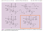
I am using a bootstrap circuit to boost gate signal for a flying switch where Vs is not grounded. The circuit is attached. I used the same one as suggested by Razavi in his paper (https://ieeexplore.ieee.org/document/7258484/ )

I used minimum W/L sizes 1.5/0.6 (I'm using C5 CMOS technology) and CL=250pF and C=100f F for the bootstrap circuit, However, when I apply Vs=15V for testing the circuit, it seems there is something wrong. The waveforms are also attached, the main switch sees Vgs=5V across the its gate-source terminals but it is turning on fully, Vd is not the same as Vs. Any hint why this is the case? I was expecting the that transistor will turn-on fully and connect Vs to Vd

Thanks in advance,
 

Attachments

  • Bstr_circuit.png
    Bstr_circuit.png
    30 KB · Views: 129
  • Bstr_waveforms.png
    Bstr_waveforms.png
    105 KB · Views: 129

Your gate voltage only exceeds Vd (which will really
act as source) by maybe 1.5V and this will form a
pretty weak channel. If CL is fat then you may see
little or no movement. Look at real Vgs and Vgd.
Also beware that if you use extended-drain or
LDMOS devices "upside down" their drain drift region
becomes a source resistance with bad impact to Ron.

Can't see values to say whether your switch is just
undersized for the load. Can't see the Razavi paper
referenced because screw IEEE and their pay wall.
 
Your gate voltage only exceeds Vd (which will really act as source) by maybe 1.5V and this will form a pretty weak channel. If CL is fat then you may see little or no movement. Look at real Vgs and Vgd.

shouldn't be the concern only Vgs? I thought if the switch sees Vgs of 5V then it turns-on fully. am I missing something here?

Also beware that if you use extended-drain or LDMOS devices "upside down" their drain drift region becomes a source resistance with bad impact to Ron.

I am using standard nMOS, so I believe this is not a problem in my case

Can't see values to say whether your switch is just
undersized for the load. Can't see the Razavi paper
referenced because screw IEEE and their pay wall.

The bootstrap transistors, Mn1-Mn4 and Mp1 & Mp2 are sized equally 1.5um/0.6um and I am using 0.1pF cap for bootstrapping. The switch transistor that I am driving is sized 21um/0.6um and CL= 250pF,

I attached a screenshot of Razavi bootstrap circuit (d in the figure, in red rectangle) which I am using,

BTW: I wanted to share the whole paper but I thought there maybe a problem in copyright. would that be an issue?
 

Attachments

  • Razavi_bstr_ckt.png
    Razavi_bstr_ckt.png
    75.7 KB · Views: 103

You show Vs at 15V, Vd at 4V and Vg pulsing 0 - 5.5V.
So best case, Vgs (=Vg-Vd) is 1.5V worth of "on" (and
gate overdrive is that, less VT).
 
You show Vs at 15V, Vd at 4V and Vg pulsing 0 - 5.5V. So best case, Vgs (=Vg-Vd) is 1.5V worth of "on" (and
gate overdrive is that, less VT).

thanks for elaboration, but I'm still not clear about why you consider Vgd not Vgs ? because I'm bootstrapping the Vgs,

I may think of it though in one way when we consider the drain and the source terminals are symmetrical (they can be exchanged) which is the case in my circuit, so we usually look for the lowest Vgs or Vgd potential . what do you think?

Actually, this circuit is one case of my whole circuit where I have 10 flying switches. when I applied bootstrap as above, I barely see any difference compared to applying 5V to the gate directly. I was expecting to see the transistor switch turns on fully
 

Still you need Vg above one of the terminals by some
volts. The lower of S, D in this case looks like D, at
~+4V.

Not sure how the CL node (D) ever got to 4V but it
sure seems uninterested in going higher.

Maybe set up simpler, with just the switch FET, its
+15V and CL, and drive the gate with a 0-5V pulse
source that has its return (-) tied to CL rather than
gnd! Then you can see what the FET switch does
when fully (-ish) driven. It may be that the on
resistance of the smallish (21/0.6) FET is too high
to meaningfully move the 250pF capacitance (at
least, with low gate drive). I know that there
would be a lot more width than that, for a digital
output buffer expecting a smaller load, generally.

21/0.6 means you're using a 5V device but you
have a 15V supply, no?
 

Still you need Vg above one of the terminals by some volts. The lower of S, D in this case looks like D, at ~+4V.

Not sure how the CL node (D) ever got to 4V but it sure seems uninterested in going higher.

Maybe set up simpler, with just the switch FET, its +15V and CL, and drive the gate with a 0-5V pulse source that has its return (-) tied to CL rather than gnd! Then you can see what the FET switch does when fully (-ish) driven. It may be that the on resistance of the smallish (21/0.6) FET is too high to meaningfully move the 250pF capacitance (at least, with low gate drive). I know that there would be a lot more width than that, for a digital output buffer expecting a smaller load, generally.

21/0.6 means you're using a 5V device but you have a 15V supply, no?

Actually, I don't have 15V supply, this is only for me to see the effect of bootstrapping. my circuit is boost converter using switched capacitors, so 250pF is a flying cap that transfer charges to next level using flying switches. I am designing 1V to 9V boost, my gate signals are 0-5V, so that is why I want make a simulation for arbitrary higher voltage, i.e 12V it could be 9V as well, for a max output that I want to see.
Theoretically and ideally the circuit works, but obviously do you to minimal Vgs/Vgd seen by some flying switches, they experience high resistance and as such the output voltage can't exceed the gate signal level. because of that, I thought of using bootstrapping technique to overcome this. but seems it did not work ? I even increase W to higher level (~150um) to minimize the Rds but still no improvement!

- - - Updated - - -

Also one more thing, the 4v seen at the drain side is coming from the source but the switch has high resolistance that prevents the drain to be 15v. When I raise Vg to 10v, the drain follows and reaches around 9v. So basically this means the bootstrap circuit has no effect !
 

so, can we say we can't do bootstrapping in cmos circuits due to the symmetrical structure of the source/drain terminals?
 

I have noticed that the bootstrap circuit is working ok, except the case when Vsource if main switch is higher than 5V which will result in turning-off the Mn3 in the drawing. Mn3 is expected to turn-on and connect the Vsource to Vc_negative plate.

So, my question, how can I make this transistor turns on regardless of the value seen by its drain (i.e Vsource of the main switch)? I have been working in this for a week now and I want to see if there is any potential or tweaks to have this circuit operational,

Bstr_circuit.png
 

Status
Not open for further replies.

Part and Inventory Search

Welcome to EDABoard.com

Sponsor

Back
Top