bio_man
Full Member level 2
Hi,
I want to design and layout a circuit using C5 0.5um CMOS technology (https://www.onsemi.com/PowerSolutions/content.do?id=16693), this technology allowing 5V and 12V transistors, all transistors in my circuit would be rated for 15V for safety (Vout can reach 15V)
I have couple of questions,
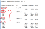
1) in the attached pic, there are difference W/L sizing ranges minimum, wide.., would you please advise me what are the main differences between them? because during my design I usually pick-up the parameters from minimum sizes. Is that a usual practice?
2) when they say the technology support 5V and 12V transistors, do they mean the rating of these transistors? in others words, would these transistors break after their Vds exceeds these voltage levels?
3) how can I differentiate between standard transistors (low voltage 5V or so) and high voltage transistors (12V)? I checked Cadence, the only difference in Schematic is the gate length, for standard nMOS the L_min=0.6um while in high voltage nMOS (nmos_hv) it's 0.9um. Does this mean in the layout I need only to play with the length? or their any other process need to be done in the layout end?
I want to design and layout a circuit using C5 0.5um CMOS technology (https://www.onsemi.com/PowerSolutions/content.do?id=16693), this technology allowing 5V and 12V transistors, all transistors in my circuit would be rated for 15V for safety (Vout can reach 15V)
I have couple of questions,
1) in the attached pic, there are difference W/L sizing ranges minimum, wide.., would you please advise me what are the main differences between them? because during my design I usually pick-up the parameters from minimum sizes. Is that a usual practice?
2) when they say the technology support 5V and 12V transistors, do they mean the rating of these transistors? in others words, would these transistors break after their Vds exceeds these voltage levels?
3) how can I differentiate between standard transistors (low voltage 5V or so) and high voltage transistors (12V)? I checked Cadence, the only difference in Schematic is the gate length, for standard nMOS the L_min=0.6um while in high voltage nMOS (nmos_hv) it's 0.9um. Does this mean in the layout I need only to play with the length? or their any other process need to be done in the layout end?
") but my point was to understand what Voltage difference does foundr refer to when they say 'the technology support 5V, 12V devices'. I thought, this is only for gate signals (Vgs), so maybe it's ok to have my transistors exposed to 15V Vds at some point. but now it is clear as pelmiras mentioned earlier, all voltages in the transistor need to be rated for these levels (5V for standard and 12V for hv ones)
but my point was to understand what Voltage difference does foundr refer to when they say 'the technology support 5V, 12V devices'. I thought, this is only for gate signals (Vgs), so maybe it's ok to have my transistors exposed to 15V Vds at some point. but now it is clear as pelmiras mentioned earlier, all voltages in the transistor need to be rated for these levels (5V for standard and 12V for hv ones)