pancho_hideboo
Advanced Member level 5
- Joined
- Oct 21, 2006
- Messages
- 2,847
- Helped
- 767
- Reputation
- 1,536
- Reaction score
- 733
- Trophy points
- 1,393
- Location
- Real Homeless
- Activity points
- 17,490
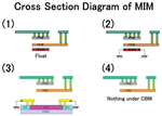
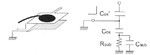
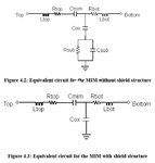
We can not ignore RF Loss from Bottom Plate of MIM Capacitor to substrate of Silicon(Psub).
I would like to reduce this loss.
My application of MIM is RF DC block Capacitor for input of 900MHz RFID Rectifier.
See attached figure where I show four structures.
RF signal is inputed to Top Plate and Bottom Plate is connected to Rectifier input.
Which is better regaring RF Loss from Bottom Plate ?