Continue to Site

Welcome to EDAboard.com

Welcome to our site! EDAboard.com is an international Electronics Discussion Forum focused on EDA software, circuits, schematics, books, theory, papers, asic, pld, 8051, DSP, Network, RF, Analog Design, PCB, Service Manuals... and a whole lot more! To participate you need to register. Registration is free. Click here to register now.

How do I design this darn differential amplifier?!

Status
Not open for further replies.

isaac12345

Member level 2
Joined
Mar 24, 2010
Messages
47
Helped
0
Reputation
0
Reaction score
0
Trophy points
1,286
Activity points
1,634
Hi all!

Been trying to design a differential amplifier with the following specifications(in cadence virtuoso) but been unsuccessful again and again. Given up! Can anyone give it a try and explain(with a schematic?). Would much appreciate it :)

Specs -

Av =>40db
Pd<100uW
Slew Rate=>20v/usec
CMRR=>50db
ICMR=0.8 to 3.0v
Gain Bandwidth product = 50MHz
Vout swing =0.7 to 1.5v

Assume load capacitance = 1pF, Vdd=2.2v, unCox=300u and upcox=50u
 

ICMR=0.8 to 3.0v @ Vdd=2.2v --- are you sure?

Show what you already have designed! Which spec didn't you meet?

Which process?
 
ICMR=0.8 to 3.0v @ Vdd=2.2v --- are you sure?

Show what you already have designed! Which spec didn't you meet?

Which process?

Sorry. I think we can suppose that Vdd is 5v.Will that affect power dissipation?

I'm stuck at the schematic simulation in cadence virtuoso. Dont have access to the computer for the next few days where the schematic is stored but safe to say its a mess of an attempt by a beginner.

Can you post the schematic and more importantly how you went about designing it?

- - - Updated - - -

Jut confirmed icmr is 0.8 to 2.0 v @vdd= 2.2v
 

I think we can suppose that Vdd is 5v.Will that affect power dissipation?
Is this a serious question, really?

I'm stuck at the schematic simulation in cadence virtuoso. Dont have access to the computer for the next few days where the schematic is stored but safe to say its a mess of an attempt by a beginner.
Show it anyway, after you get access. Or a drawing of your design, at least.

Can you post the schematic and more importantly how you went about designing it?
Don't expect forum members to do your job. These forums are meant to help with special individual problems, if the thread starter shows what he's done before, and if he's willing to give enough info to help him.

Until now you didn't even respond to all the questions: which process? More exactly: which models do you use? Are you aware that the Gain Bandwidth Product (UGB) depends rather much on the load impedance? No info about this ...

- - - Updated - - -

Jut confirmed icmr is 0.8 to 2.0 v @vdd= 2.2v
Sounds better.
 

Is this a serious question, really?

Show it anyway, after you get access. Or a drawing of your design, at least.


Don't expect forum members to do your job. These forums are meant to help with special individual problems, if the thread starter shows what he's done before, and if he's willing to give enough info to help him.

Ok. Apologies. It just that this circuit's been doing my head in for the past few days!

Until now you didn't even respond to all the questions: which process? More exactly: which models do you use? Are you aware that the Gain Bandwidth Product (UGB) depends rather much on the load impedance? No info about this ...

No I dont know which model. All I know is that I am using cadence virtuoso to simulate it and doing pen and paper calculations. Like I said, i'm quite the beginner to this. Are there any good video lectures that I could refer to? How's this one? -https://www.youtube.com/watch?v=4qpVtZnf0eg
 

Not too bad, I think ;-)

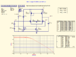
Now here's sort of a suggestion for your diff-amp. As you didn't provide any info about your process/models/threshold voltages, I had to use my own. They're from a 0.18µm process; I assumed a load capacitance of 1pF :

180nm-1-stage-OTA-50MHz-1pF-ICMR.png

Note: Presumably, your process, especially your models might be quite different from mine, so it's predictable that you'll attain rather different results. Hence consider my above suggestion just as a first trial for your design, then try and optimize to achieve your specs.

Also pls. note that my simulations are based on schematics (pre-layout), and that post-layout simulations (if you need to generate a layout) will obviously result in a considerable lower fT (gain-bandwidth product), due to parasitics.
 
Not too bad, I think ;-)

Now here's sort of a suggestion for your diff-amp. As you didn't provide any info about your process/models/threshold voltages, I had to use my own. They're from a 0.18µm process; I assumed a load capacitance of 1pF :

View attachment 141400

Note: Presumably, your process, especially your models might be quite different from mine, so it's predictable that you'll attain rather different results. Hence consider my above suggestion just as a first trial for your design, then try and optimize to achieve your specs.

Also pls. note that my simulations are based on schematics (pre-layout), and that post-layout simulations (if you need to generate a layout) will obviously result in a considerable lower fT (gain-bandwidth product), due to parasitics.

Nice! Very neat! Which software did you use to draw and simulate the circuit?
 

Hello,
I0 is reference current?
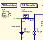
and how you measured the power dissipation?


How is the software compared to Cadence Virtuoso? Is it a decent substitute?

2. And how did you go about designing the circuit? Where did you start from?

3. What's V1dc and I0 for?

4. What's DC1 for?

5. What's M3's function?

6. How do I get good at analog electronics?

Thanks :)
 
Last edited:

Where did you start from?

The differential amplifier begins with a long-tail pair. Its behavior is not readily obvious just by looking at the schematic. If you increase current through the left side, it has the effect of reducing current in the right side. And vice versa.

Try first experimenting with the long-tail pair by itself, to get an idea how it works. See what supply voltages work, as combined with input voltages. Later you can add the other sections of your amplifier.
 

I0 is reference current?
It's a bias current. By M1 multiplied by 4 for the 2 branches.

how you measured the power dissipation?
By multiplying V0's voltage with Pr1's current value. power-dissipation.png


How is the software compared to Cadence Virtuoso? Is it a decent substitute?
A moderate substitute, I'd say, but free software. At least it involves a SPICE-like simulator. Problem is to integrate the models.

2. And how did you go about designing the circuit? Where did you start from?
From your specs.

3. What's V1dc and I0 for?
V1dc constitutes the ICM voltage. Stepped by a DC simulation sweep. For I0 s. above.

4. What's DC1 for?
DC1 is the name of the DC simulation (for the stepped ICMR simulation).

5. What's M3's function?
It's the master of the M3->M1 current mirror.

6. How do I get good at analog electronics?
Study Analog Circuit Design textbooks, YouTube presentations on this stuff, and follow the thread explanations in this forum!
 
It's a bias current. By M1 multiplied by 4 for the 2 branches.

By multiplying V0's voltage with Pr1's current value. View attachment 141492


A moderate substitute, I'd say, but free software. At least it involves a SPICE-like simulator. Problem is to integrate the models.


From your specs.


V1dc constitutes the ICM voltage. Stepped by a DC simulation sweep. For I0 s. above.


DC1 is the name of the DC simulation (for the stepped ICMR simulation).


It's the master of the M3->M1 current mirror.


Study Analog Circuit Design textbooks, YouTube presentations on this stuff, and follow the thread explanations in this forum!

Great reply!

I tried coming up with same circuit from the video tutorial I linked to above but couldnt get it. How did you go about deriving the various values(equations,calculations,etc)?
 

I = C•δV/δt = 1pF•20V/µs = 20µA
 

Status
Not open for further replies.

Similar threads

Part and Inventory Search

Welcome to EDABoard.com

Sponsor

Back
Top