guitardenver1
Newbie level 4
I have a transimpedance amplifier circuit for a photodiode. The circuit is below.

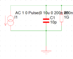
There are other parts in this circuit as well. There is the photodiode, analog switch and another non-inverting gain stage that has a digital pot on the feedback resistor.
The photodiode model is below:
The Analog switch with input and output capacitance, series resistance and on leakage current is below:
Switch P# = SN74LVC1G66DCKR

Gain stage with digital pot is below. Digital pot is circled in red:
Digital Pot P# is MCP4011-103E/SN

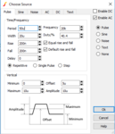
Here is the simulation parameters of the photodiode current source:
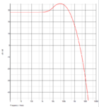
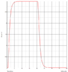
Here is the output of the simulation:
Questions:
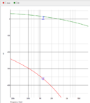
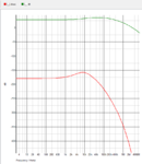
1) If I put a phase plot to the output, it looks like the circuit is unstable since the phase starts at -180deg and there is gain greater than 1 when it goes below -180. Is this circuit really unstable or am I reading it wrong?
2) I want to add a high pass filter to the design to filter out low frequencies. I am only interested in pulses between 7uS and 20uS. Where would this best be achieved? Before or after the 2nd gain stage? I would be ok with a -3db point at 10kHz on the low end and a -3db at 1MHz on the high end.
3) Am I modeling the analog switch correctly?
ADIsimPE Simulation file is attached.

There are other parts in this circuit as well. There is the photodiode, analog switch and another non-inverting gain stage that has a digital pot on the feedback resistor.
The photodiode model is below:

The Analog switch with input and output capacitance, series resistance and on leakage current is below:
Switch P# = SN74LVC1G66DCKR

Gain stage with digital pot is below. Digital pot is circled in red:
Digital Pot P# is MCP4011-103E/SN

Here is the simulation parameters of the photodiode current source:

Here is the output of the simulation:


Questions:
1) If I put a phase plot to the output, it looks like the circuit is unstable since the phase starts at -180deg and there is gain greater than 1 when it goes below -180. Is this circuit really unstable or am I reading it wrong?

2) I want to add a high pass filter to the design to filter out low frequencies. I am only interested in pulses between 7uS and 20uS. Where would this best be achieved? Before or after the 2nd gain stage? I would be ok with a -3db point at 10kHz on the low end and a -3db at 1MHz on the high end.
3) Am I modeling the analog switch correctly?
ADIsimPE Simulation file is attached.
