shaiko
Advanced Member level 5
Hello,
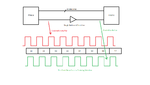
FPGA A is connected to FPGA B via a source synchronous parallel bus - 8 data lines and 1 clock.
FPGA A asserts data with a tco of 0.5ns from the positive clock edge to data valid.
However, the system has a design flow: The clock line that connects FPGA A and B is passed through a buffer while the data lines don't.
This buffer causes the clock to be delayed for 2 ns - essentially changing the tco FPGA B sees to a negative value.
I solved the problem with a PLL via changing the phase of the input clock to a safe value.
But can such problem be solved via SDC only ?
I.E: tell the timing tools that I'm expecting a negative propagation delay and have it solve the problem...