Continue to Site

Welcome to EDAboard.com

Welcome to our site! EDAboard.com is an international Electronics Discussion Forum focused on EDA software, circuits, schematics, books, theory, papers, asic, pld, 8051, DSP, Network, RF, Analog Design, PCB, Service Manuals... and a whole lot more! To participate you need to register. Registration is free. Click here to register now.

What considaration should be taking into account in gating rather remote Power IGBT?

Status
Not open for further replies.

kappa_am

Full Member level 6
Joined
Jul 16, 2012
Messages
331
Helped
19
Reputation
38
Reaction score
19
Trophy points
1,298
Location
Vancouver
Activity points
3,859
Hi all,
I am using 3 SKHI22B drivers to fire a 75A, 1200V IGBT brick (3 phase). Unfortunately, there is no way to shorten the distance between driver and the module brick (it's about 30cm). I am afraid that this length would lead to a problem ( oscillating with gate capacitor, causing IGBT works in the linear region...).
I would be grateful if you share your idea to minimize the effect of the connection wire on the firing and IGBT performance.

Thank you
 

Hi,

I recommend to avoid this. Remember 30cm in one direction and 30cm back. I wonder why you need the driver to be 30cm away.

Usually with such situations I recommend a twisted wire. Directely to gate and emitter. But I doubt it could be made with a properly terminated system. But you don't need a two wires, but three wires...

May I ask why you can't put the driver circuit closer to the IGBTs?

Klaus
 

A gate reference with negative bias voltage should keep device far from linear region.
 

Thank you for your response.
It is a packaging restriction.
actually, IGBT brick is mounted on the heat sink; beside it, I have two small PCBs mounted one above the other, then the Driver board which includes driver mounted the top of the upper board. It is large and covers all heat sink so I need lift it above capacitors etc and consider safe distance between board and capacitor terminals.
The driver connects to the IGBT by 3 wires, since it has fault detection feature. I think a resistor between gate and drain is mandatory.

- - - Updated - - -

SKHI2B has -6V reference. But I am worried about ramping time of gating signal. Also, oscillation and other weird phenomena happen when parasitic inductance and or capacitance exist.
 
Last edited:

I think a resistor between gate and drain is mandatory.
Resistor between gate and drain?

30 cm cable sounds feasible. I see that Semikron suggests 22 ohm gate resistors for 75A IGBT. They should already achieve an aperiodic damping for 30 cm twisted pair. But it's recommended to check the actual switching waveforms and adjust the gate resistors if necessary.

If the inductance of a single twisted pair is too high, multiple parallel connected pairs can be a solution.
 

Thanks for the guidance. My bad, I meant gate-source.What about drain connection? it should be left alone or all three connection should be twisted around each other?
 

Drain sense inductance is less critical and the wire must not necessarily be closely twisted with the other wires. But it's O.K. to have the three in a cable.

If you don't place the series diodes at the IGBT side, you need 1000 V isolation for the drain sense against gate and source wires.
 

Thank you. I will try it.
another doubt I have is that since the distance of capacitor bank and the IGBT brick is about 20cm, I have put a film capacitor in parallel with electrolytic capacitors right on the IGBT brick's DC terminals. Do you think this is enough for snubber purpose or I need separate snubber for each switch? ( application is IM drive two-level -3-phase inverter, diode rectifier front, and will be active front end in some applications).
 

Something that has worked (for me at least) when designing high power circuits, is to always have duplicate protections, to be very conservative with snubbers and bypass capacitors, and make every effort to lower drive impedances.

Afterwards, and only after I have fully validated the design with rigorous measurements and testing, then I start *Muntzing* the circuit.

https://en.wikipedia.org/wiki/Muntzing
 

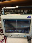
I have built the setup, but there is a strange phenomenon on the DC link caused by IGBTs which generates noises and stops SPI communications on the nearby circuits. Please look at DC bus voltage in below picture. (the load is a motor but stopped. the duty cycle of upper and lower switches of the inverter is 50%). What's the problem? ringing? what can I do? the gate wires are twisted, 10k gate-source resistance, the driver is SKHI22B and the distance between driver and the gate is about 25cm, and DC link voltage is 300V.

Thank you for your comments.

IMG_20171016_173443379.jpg
The probe is *10.
 

Status
Not open for further replies.

Similar threads

Part and Inventory Search

Welcome to EDABoard.com

Sponsor

Back
Top