Continue to Site

Welcome to EDAboard.com

Welcome to our site! EDAboard.com is an international Electronics Discussion Forum focused on EDA software, circuits, schematics, books, theory, papers, asic, pld, 8051, DSP, Network, RF, Analog Design, PCB, Service Manuals... and a whole lot more! To participate you need to register. Registration is free. Click here to register now.

MOS switches / transmission gates

Status
Not open for further replies.

CAMALEAO

Full Member level 4
Joined
Jul 29, 2016
Messages
201
Helped
2
Reputation
4
Reaction score
2
Trophy points
18
Activity points
1,868
Hi everyone,

I have a question regarding mos switches. Is there any rule of thumb on designing mos switches? To things like charge injection, having the lowest resistance as possible, avoid spikes during turn on, etc?

For example, something that comes into my mind is having the pmos W 3 times the size of nmos.

Best regard.
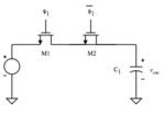
 

charge injection: to minimize it, put the same short-circuited anti-phase controlled transistor in series:
minimize_charge-injection.png

lowest resistance as possible: No. Just the right resistance. Calculate it via the voltage division between switch and load, or for the necessary highest transmission frequency f = 1/2πRC for capacitive load C .

spikes during turn on: will be minimized by charge injection minimization (s. above)

pmos W 3 times the size of nmos: depends on process/PDK. This factor should be equal to the ratio of the low-field channel carrier mobilities µ0n/µ0p for n- / p-channel MOSFETs.
 

Charge injection cancellation can be tricky, the Qinj
depends on both the capacitance and the common
mode position (dQ=CdV, neglecting the nonlinearity
of C) and where the M1 (ref above post) gate charge
goes, on turnoff, is also pretty variable with the
internal and external impedances, as far as the
partitioning of gate charge between S, D, B.

In the above example, M2 supplies (Cgs+Cgd)*dVph1_
but M1 may push only Cgd*dVph1 toward C1, with
Cgs*dVpgh1 going back out the input. This might
-overcompensate- the charge injection. This can
be tweaked, and it may be better to use two half
(*) FETs, one before and one after the switch.

* give or take - tweak ratio to suit, given expected
application and test conditions

In designing S/H products I've found it useful to
make adaptive switch gate drive that takes the gate
to no more negative (N) or positive (P FET) than it
takes to get to "off". This minimizes "off" transition
overtravel and C*V charge. Of course then you need
level shifters and biases and on chip decoupling, and
all of that has to slew with the input voltage (so a
buf amp at minimum and had better track and settle
fast).

Re on resistance, classical low field mobility ratio is
not the whole deal in modern, highly "drain engineered"
MOS technolgies - the on resistance may be dominated
or at least significantly bent by the LDD and halo regions
which act as minuscule JFETs in series with source and
drain. In a "digital" flow you are almost certain to see
this (some RF and analog flows offer a non-extended
"analog" device that gives better linearity and lower on
resistance, at perhaps the cost of longer min L or lower
application voltage rating). You probably want to tune
by simulation, provided that you believe the foundry
device models are decently fitted for both channel and
access (extension*halo) behavior.
 

There is a trade-off between low resistance (low Rdson --> low DC power loss) and low capacitance (low dynamic power loss C*f*V^2).

Other things that might be important, depending on applications:

1. gate resistance and switching uniformity - for low Rdson / lareg area devices (gates should not be too wide, to avoid distributed effects and voltage drop and delay along the gate width).

2. drain dV/dt effect - when device is turned off, a fast ramp of Vds is charging the gate through Cgd, which can dynamically open gates (above Vt), causing a shoot-through current and hence a loss of efficiency.
Value of Cgs and ratio of Cgs to Cgd is important here, as well as the gate resistance.

3. Current peaking during switching - often caused by parasitic inductance, in power loop and gate loop.
Careful layout, and placement of decoupling capacitor is important.

4. For high current devices - avoid current crowding and current imbalance.
Current densities should stay within design rule values.
 

lowest resistance as possible: No. Just the right resistance. Calculate it via the voltage division between switch and load, or for the necessary highest transmission frequency f = 1/2πRC for capacitive load C .
Please explain more about just the right Rds_on and voltage division ???
 

Just the right resistance. Calculate it via the voltage division between switch and load, ...

Please explain more about just the right Rds_on and voltage division?

In general: vout/vin = Zout/(Zin+Zout)

An example: if you want to transfer 90% of the voltage level value via the switch, its

• Rds_on(switch) must be Rload/9
or
• Cswitch must be 9*Cload
 

Status
Not open for further replies.

Part and Inventory Search

Welcome to EDABoard.com

Sponsor

Back
Top