Continue to Site

Welcome to EDAboard.com

Welcome to our site! EDAboard.com is an international Electronics Discussion Forum focused on EDA software, circuits, schematics, books, theory, papers, asic, pld, 8051, DSP, Network, RF, Analog Design, PCB, Service Manuals... and a whole lot more! To participate you need to register. Registration is free. Click here to register now.

Buck convertor my circuit has been damaged

Status
Not open for further replies.

baby_2

Advanced Member level 4
Joined
Jul 20, 2016
Messages
105
Helped
2
Reputation
4
Reaction score
1
Trophy points
18
Activity points
873
Hi,
Here is my circuit
SMPS-basic-2.gif
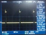
I use a IGBT(VCE>800 , IC=35) instead of BJT transistor with a IGBT driver(VCC=15v). I want to get a 1A current output with switching frequency 50khz (duty cyle less than 15%).
However after I inject 220VAC as input my IGBT gone and after that all my circuit behind of gate such as IGBT driver , PWM generator has gone too.
what is my mistake?
 

Hi,

what is my mistake?
* wrong PCB layout
* wrong device selection
* wrong schematic
* ..

Klaus
 
  • Like
Reactions: baby_2

    baby_2

    Points: 2
    Helpful Answer Positive Rating
Most likely problem is with the gate drive circuit, which isn't shown. Show your full schematic if you really want help.

Also consider testing with a lower voltage/current supply, rather than just plugging it into the wall first.
 
  • Like
Reactions: baby_2

    baby_2

    Points: 2
    Helpful Answer Positive Rating
Thanks a lot for your comment
Here is my gate driver (10 ohm resistor is series with gate) and I make a clear and exact pwm wave form with my micro-controller
Untitled.png
 

Hi,

What is "TC442"?
Without power supply it won´t work.
Without capcitors it won´t run stable.
Without proper layout it won´t run stable.

I´l be back when there is useful information.

Klaus
 

TC4426 is a low side driver. How is the driver supply connected input DC and how the pwm signal to the gate driver?

You need a floating power supply for the driver and isolation for the pwm signal.
 
  • Like
Reactions: baby_2

    baby_2

    Points: 2
    Helpful Answer Positive Rating
Hi,
Thanks for your contributions
Here is my IGBT driver circuit ( I applied 15v for biasing the driver and also a 10ohm series resistor in gate pin) (TC4426)
Capture.PNG
the PWM generates with micro-controller that you can see the output pwm wave form after passing the driver (at gate) here
 

My output voltage is 40volt
 

As expected, the problem is with the unsuitable gate driver. As FvM stated already, the TC442 is a low side gate driver, but you're using a high side switch. Consider using a proper high side gate driver (IR2110 family), or using a P channel device with proper driver circuits.
 
  • Like
Reactions: baby_2

    baby_2

    Points: 2
    Helpful Answer Positive Rating
Consider using a proper high side gate driver (IR2110 family), or using a P channel device with proper driver circuits.
Or, he can move the IGBT in the low side and still use the current low-side gate driver, but then, the load will float.
 
  • Like
Reactions: baby_2

    baby_2

    Points: 2
    Helpful Answer Positive Rating
Thanks for your recommendation and explanation
I've used 2101 with this circuit.
Capture.PNG

I inject a %20 PWM voltage (20% on) but I get output voltage ( I put a resistor at the output) with average of 10v!! and when I change duty cycle to %80 I get 7V across the output resistor.
 
Last edited:

Hi,
My problem is that I can't get less voltage with changing pwm duty cycle less than 10% but as I know with duty cycle between 0 to 100% I should get the minimum and maximum voltage across the load. it means my MOSFET doesn't switch on or off completely.
 

In buck converter it is not advisable to go for less than 10% duty cycle. Device strain will be substantially higher.
 
  • Like
Reactions: baby_2

    baby_2

    Points: 2
    Helpful Answer Positive Rating
In buck converter it is not advisable to go for less than 10% duty cycle. Device strain will be substantially higher.
Don't agree as a general rule. Buck converters with low duty cycle are less efficient, switching losses (and "device strain") are proportional to input voltage multiply output current in the first order. But there are cases where 5 % or even lower duty cycle is appropriate for designed fixed output voltage. Furthermore it's just normal to have switchers with variable output voltage starting at zero.

A bootstrap gate driver as used in the present circuit will however never work with 100 % duty cycle, and it may also have problems with very low duty cycle and startup without a resistive load. The driver is intended to be used with synchronous (transistor/transistor) switchers and has problems with transistor/diode switchers.
 
  • Like
Reactions: baby_2

    baby_2

    Points: 2
    Helpful Answer Positive Rating
Status
Not open for further replies.

Similar threads

Part and Inventory Search

Welcome to EDABoard.com

Sponsor

Back
Top