Continue to Site

Welcome to EDAboard.com

Welcome to our site! EDAboard.com is an international Electronics Discussion Forum focused on EDA software, circuits, schematics, books, theory, papers, asic, pld, 8051, DSP, Network, RF, Analog Design, PCB, Service Manuals... and a whole lot more! To participate you need to register. Registration is free. Click here to register now.

IO Pads Layout Tips .

Status
Not open for further replies.

bio_man

Full Member level 2
Joined
Mar 30, 2010
Messages
144
Helped
2
Reputation
4
Reaction score
4
Trophy points
1,298
Activity points
2,698
hi,

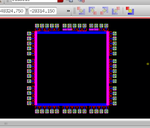
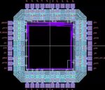
I am using CN05 Technology and I got PadFrame (attached) from a friend who used to layout digital IC. For my IC, I have Comparators on-board. My questions:

1) Should I care too much about the Pad type ( digital vs. analog)?
2) The PadFrame I got looks very simple not like others I saw in Literature (example of a Pad is also attached), Is it OK?
3) For one input to my circuit, I want to sense a small voltage (0.3-0.5 V) that comes from an off-chip solar cell, is it ok to ignore the ESD protection for this Pad? because I dont't want the ESD circuit to distort this small voltage signal.
4) Can you please advise how can I check the acceptable thickness of my traces that can handle current of the circuit?


Thanks all

- - - Updated - - -

Update: my circuit contains a ring oscillator that generates 500kHz internally
 

Attachments

  • Pad_myIC.png
    Pad_myIC.png
    64.1 KB · Views: 218
  • Pad_litrature.jpg
    Pad_litrature.jpg
    141.4 KB · Views: 1,185

The ESD steering diodes are unlikely to leak more
than pA (room temp) and nA (hot). You are probably
at liberty to design customized ones but I'd take
lessons from anything that looks "blessed" (like,
has a purported ESD model* withstand_voltage
rating).

You need to look at the "guts". A digital input
pad is likely to have a 2-layer ESD network with
a fat front end diode pair, a series resistor in the
tens of ohms (or maybe even low hundreds) and
a "backstop" diode pair inboard at the first inverter
gate node. This is fine for inputs that don't have
DC current. Maybe not-fine for analog, depending.

Digital output and bidirectional pads have fat
driver FETs attached and will see MOS leakage
(>= diode leakage) at the pin.

Analog pads I'd expect to be direct connect,
shunt diodes only. These are what I'd use (but
know your toolbox, open the lid).

There are numerous pad-frame styles. The one
at left in the thumbnails looks to have multiple
chip scale power busses, on the right maybe
only two. I often like to route the ground bus
outboard of the pads and bury ground returned
clamp and drive elements under it. But all together
is pretty normal.

There should be technology documents that
assert a reliable current carrying capacity for
conductors, every layer, mA/um. For industrial
temp range I'd say rule of thumb, 1mA/um for
thinner lower interconnect levels, maybe up to
5mA/um for (say) 3um thick top metal. But
look through the reliability rules section of PDK
docs. Lower if you want MIL or higher temp.

You want some decent on chip decoupling for
your ring oscillator, independent of the main
chip. Supply noise can corrupt or make fail,
ring oscillators and this goes for self-generated
noise as well. I'd resistor-isolate the osc core
from the rails and put a fat bank of MOS caps
(which I'd draw as L=5, W=10-ish multifinger
with contacts at each gate end strapped by Met2
slab, while Met1 slab hits all the S/D stripes in
between). Analyze this entire (osc + Cdecouple)
circuit with large inductors in series with the power
supply and verify that the decoupling suffices for
all AC / edge rate needs. At the first buffered
stage (not core loop) cross to the main supply
domain for any further drive gain.

I've had ring oscillators fail to measure at probe
due to these sorts of environment issues, but work
OK in package with colse-in decoupling. On chip is
best. May also, if you plan to test, put series
resistors in any output-to-eqpt path to keep the
current impulses down.
 
dick_freebird you have been so helpful, I usually learn a lot from your responses\experience. thank you so much!

Regarding the PadFrame, it looks like they occupy 40-60% of die size, right? For example, I measure the one in the left, it occupies 1.76mm2 on my 4mm2 die.

You want some decent on chip decoupling for your ring oscillator, independent of the main chip. Supply noise can corrupt or make fail, ring oscillators and this goes for self-generated noise as well. I'd resistor-isolate the osc core from the rails and put a fat bank of MOS caps (which I'd draw as L=5, W=10-ish multifinger
with contacts at each gate end strapped by Met2 slab, while Met1 slab hits all the S/D stripes in between). Analyze this entire (osc + Cdecouple) circuit with large inductors in series with the power supply and verify that the decoupling suffices for all AC / edge rate needs. At the first buffered stage (not core loop) cross to the main supply domain for any further drive gain.

I've had ring oscillators fail to measure at probe due to these sorts of environment issues, but work OK in package with close-in decoupling. On chip is best. May also, if you plan to test, put series resistors in any output-to-eqpt path to keep the current impulses down.

for my ring oscillator, it gets supplied from the solar cell (0.3-0.5V Voc) then using series of charge pumps this voltage is boosted to higher level (~1V) which will be used to startup the control circuits that include all logic gates and comparators. This operation is verified in schematic simulation and I am doing the layout right now. With this being said, don't you think connecting Caps or resistors on the path of ring oscillator supply would effect the oscillation process?

May also, if you plan to test, put series resistors in any output-to-eqpt path to keep the current impulses down.

would you please elaborate on what you mean by output-eqpt path?
 

1) yes, absolutely. digital pads will typically output full swing logic (0->core VDD), it doesn't look like that is what you want. You want analog pads, for at least a portion of the IO ring.
2) the image on the right is missing layers/reference cells. I assume once you draw it with all layers/cells, it will look very similar to the one on the left.
3) check your documentation. you can let the ring take care of ESD for you or you have to build ESD protection scheme yourself, depending on what your IP offers. the former is much easier than the latter.
4) which traces? the ones internal to the chip that form the core ring? you can use some hand-wavy estimation for that, assume current comes equally from all 4 sides and figure out the metal width from that.
 
2) the image on the right is missing layers/reference cells. I assume once you draw it with all layers/cells, it will look very similar to the one on the left.

what is meant by reference cells?
Also what IP stands for? you mean PDK?
 

IP is "intellectual property". In this case it means the
pre-existing cell, device and paraphernalia libraries the
foundry may have provided for free or for fee (the low
level stuff is often "enablement" but more complex art
is provided under a $ license, from foundry or third
parties). I/O libraries are one such.

By output-eqpt path, I mean things like the RO output
to oscilloscope for measurement - a typical probe will
add >10pF to the node, a 1V/1nS signal risetime (not
unreasonable at all for 5V) means a ~ 2.5nS FWHM,
10mA "punch in the gut" for the RO (supplies may be
too inductive, through the harness and fixturing and
so on, to flatten it).

You can trade rolled-up intrument bandwidth for a
lesser impulse current (and collateral effects) by
putting a series resistor between chip and probe.
Corner freq = Rseries*10pF more or less. The
500kHz fundamental would tolerate maybe a 50K
series res, a 5K would pass the first 4 odd harmonics
(preserving square wave shape more or less) but
limit peak current to below 1mA (if 5V swing, which
it probably isn't). It's a thing to try, if RO seems to
fail every time you put the probes to it. Signal may
be degraded in amplitude, might need to "cal-map"
your setup if you care about amplitude but you can
at least measure frequency (if that's the plan).
 
Status
Not open for further replies.

Part and Inventory Search

Welcome to EDABoard.com

Sponsor

Back
Top