Continue to Site

Welcome to EDAboard.com

Welcome to our site! EDAboard.com is an international Electronics Discussion Forum focused on EDA software, circuits, schematics, books, theory, papers, asic, pld, 8051, DSP, Network, RF, Analog Design, PCB, Service Manuals... and a whole lot more! To participate you need to register. Registration is free. Click here to register now.

Power on Reset (POR), vdd range 1.6V~3.6V NEED HELP

Status
Not open for further replies.

Cesar2017

Newbie level 4
Joined
Jul 7, 2017
Messages
5
Helped
0
Reputation
0
Reaction score
0
Trophy points
1
Activity points
45
I was asked to design a Power on Reset circuit to be able to work for supply vdd range from 1.6V~3.6V in 28nm process. I need a transistor level structure for this design.

This power on reset only has one input which is supply vdd and it's a ramping Vdd.
Take Vdd ramps from 0 V to 3.6V as example, the only output RESET should go to high when the vdd is above 2.7V(3/4 of full scale vdd) this threshold voltage. If vdd ramps from 0V to 1.6V, the only output RESET should go to high when the vdd is above 1.2V.

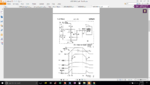
I tried to use one structure in US patent 5534804 published in 1996 as I attached, however, if I want to make sure the threshold voltage for the full scale vdd(3.6V) to be 2.7V, then this circuit only works for vdd range from 2.1V to 3.6V. I have no way to go low as 1.6V as required.

Please provide me with some useful structure, thank you guys! I have attached my structure below.
 

Attachments

  • POR_structure_1996.png
    POR_structure_1996.png
    170.1 KB · Views: 138

Sorry, one thing needs to be corrected, the range I can achieve is only from 2.8V to 3.6V, not the 2.1V I mentioned above.
 

... if I want to make sure the threshold voltage for the full scale vdd(3.6V) to be 2.7V, then this circuit only works for vdd range from 2.1V to 3.6V. I have no way to go low as 1.6V as required.

... the range I can achieve is only from 2.8V to 3.6V

Hence the supply voltage operation range (>2.8V) is above your required threshold voltage (2.7V), i.e. the RESET output is always high?
Means the circuit doesn't work at all?
 

No, 2.7V this threshold is for vdd ramps from 0V to 3.6V. 2.7V is 3/4 of 3.6V. I wanna make sure for each case threshold voltage beyond 3/4 of the vdd.
If I sizing the transistor to make this vdd 3.6V case work, then for the case vdd ramps from 0 to 3.5V, right now the threshold required is 3/4 of 3.5V which is 2.625V. it can work. In general, I for vdd ramps from 0 to 2.8, from 0 to 2.9 from 0 to 3.0, .......I can all make sure the threshold voltage for each case is beyond 3/4 of its corresponding vdd.
But when vdd is below 2.8, I mean may be ramps from 0 to 2.6V, then the Reset signal will be gone. That's why I ask for another possible structure.
 

Most Schmitt Trigger gates have 1/3 Vdd hysteresis and thus thresholds at 1/3 off and 2/3 On
you are looking for a 3/4 threshold only but unspecified off condition.

Can you use Schmittt Trigger design but non-inverting?
 

3.6V in 28nm doesn't sound right. You will have to use IO transistors for that?!
 

Hi, SunnySkyguy, thank you for your suggestion, I think that's a good idea.
One thing I'd like to make sure is that if I use schmitt trigger, the most regular structure, since my vdd is ramping from 0V to 3.6V, then the input for the Schmitt Trigger should be a division of the vdd which follows the vdd? If this is the right thought, can you suggest a structure which generate this input from the vdd so that this input follows the vdd and then I can use it as the input for Schimitter Trigger? Thank you.
 

Hi,ThisIsNotSam, I change all the transistor to be" nch_25od33_mac" this type of transistor, and the process is tsmcN28, which is correct.
 

Sounds like you want a POR release threshold which is
proportional to a future settled voltage value. As far
as I'm aware, the General Purpose Linear Anticipator
function has yet to be reduced to practice.

POR only has to wait until logic functionality can be
certain. This is more like VTN+VTP and not really about
an absolute supply level (although if you want to release
into an already-at-speed clocked condition, that might
need to be raised to the point where logic can function
-at speed-, another ballgame). Point being POR does
not often need to know the eventual supply value.
 

Hi,ThisIsNotSam, I change all the transistor to be" nch_25od33_mac" this type of transistor, and the process is tsmcN28, which is correct.

you see nothing wrong with that? what do you think those numbers (25 & 33) stand for?
 

Status
Not open for further replies.

Part and Inventory Search

Welcome to EDABoard.com

Sponsor

Back
Top