Continue to Site

Welcome to EDAboard.com

Welcome to our site! EDAboard.com is an international Electronics Discussion Forum focused on EDA software, circuits, schematics, books, theory, papers, asic, pld, 8051, DSP, Network, RF, Analog Design, PCB, Service Manuals... and a whole lot more! To participate you need to register. Registration is free. Click here to register now.

1210 footprint is too small but does it matter?

Status
Not open for further replies.
T

treez

Guest
Hello
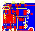
Our PCB layout contractor has placed two 1210 capacitor footprints on our PCB. The dimension of the copper on these is 4.6mm x 2.3mm (L X W) as in the attached.
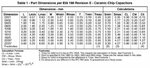
A 1210 footprint can be in worst case 2.7mm wide.
He tells us that this doesn’t matter.
Is he right? Or will our ceramic capacitors not solder properly?
 

Attachments

  • C15 C16.jpg
    C15 C16.jpg
    113.7 KB · Views: 222
  • Capacitor size table.jpg
    Capacitor size table.jpg
    96.3 KB · Views: 1,414

Hi,

I've seen this a couple times before in datasheets, that the pads for a ceramic capacitor are smaller than the package is wide.
Reliable information from big brands...therefor I assume it us OK.
But in my designs I made the smd pads wider, at least as wide as max device width.

Klaus
 

Thanks, i just tried to find what the IPC pad calculator tool gives for a 1210 capacitor and it wouldnt state it...

https://www.pcblibraries.com/LibraryExpert/

...i put in the dimensions and tolerances from the capacitor datasheet, and nothing comes up.
Do you know how to use this pad calculator tool?
 

The only time it would be a concern is on a resistor which is operating very close to its maximum power rating.

SMT resistors dissipate a significant amount of heat thru their pads, and in those instances, I would like to see a pad to be larger than the component itself.
 

Thanks, i wonder what IPC has to say about it?, especially if the outer edges of the capacitor's copper pad actually rest on the solder resist that surrounds the pad footprints?

- - - Updated - - -

I've seen this a couple times before in datasheets, that the pads for a ceramic capacitor are smaller than the package is wide.
Reliable information from big brands...therefor I assume it us OK.
Thanks, i appreciate that you yourself are wary of this, like i am too.....it leads to anomalies as follows....

If its OK to undersize chip capacitor pads, then why is it not OK to undersize microcontroller pads?
-Consider the 28UQFN recommended footprint of the PIC16F18856 microcontroller……

PIC16F18856 (footprint of UQFN on page 652)
**broken link removed**

……the pads could be undersized to a width of 0.14mm (instead of the recomended 0.2mm) so that there was a gap of 0.26mm from pad to pad. –With this sizing, it would then be possible to achieve an 80um solder resist “coast” around each pad, and then a 100um solder resist “bridge” between the pads. –This way you would guarantee getting at least some solder resist between the pads, and yet no solder resist spilling over onto the pads.
So why is undersizing not OK for a microcontroller, but OK for a chip capacitor?
 

The solder resist opening of his footprint is 2.6mm wide, so therefore, the 2.7mm wide (max tolerance) 1210 capacitors will actually be resting on the solder resist. I know its only slight, but surely this isn’t advised?
 

My view is unless you are really stuck for space use the proper IPC footprint which has a pad width of 2.7mm. Even when space is a t a premium you have to consider the component dimensions even if using least footprints.
Again I would not accept this standard of working.
 
  • Like
Reactions: treez and FvM

    FvM

    Points: 2
    Helpful Answer Positive Rating
    T

    Points: 2
    Helpful Answer Positive Rating
I have seen this before, it does work and there was a very good reason for it.

As you may already know large ceramic capacitors are prone to cracking due to thermal stresses. a capacitor manufacturer (who's name I can no longer remember, something like kemec??) did extensive research and produced white papers that proved that by having smaller pads than the width of the capacitor the stresses on the cap were greatly reduced.
The capacitors solder and are connected and physically held perfectly well with this method. Having had assembly runs in the hundreds of thousands with all ceramic caps having reduced pads no problems were ever found due to the pad dimensions. In fact many previous problems of cracked caps were greatly reduced.

However, this may not be why it was done - it may just be because he got the footprint wrong (I have seen this happen many times, both I and Marce have got footprints wrong before, no one get them right all the time. :) )

As your the customer, if the board is still in the design stage then get him to correct it with an IPC-7351B\C footprint, they are easy to make with the free library expert, so I'd expect this correction to take only about 5-10 minutes max.
If however it is too late and the board has gone to the fabricators - dont worry too much about it, a hole will not open in the ground swallowing you all - it will still work.
 
  • Like
Reactions: Garyl and treez

    T

    Points: 2
    Helpful Answer Positive Rating

    Garyl

    Points: 2
    Helpful Answer Positive Rating
Status
Not open for further replies.

Part and Inventory Search

Welcome to EDABoard.com

Sponsor

Back
Top