Continue to Site

Welcome to EDAboard.com

Welcome to our site! EDAboard.com is an international Electronics Discussion Forum focused on EDA software, circuits, schematics, books, theory, papers, asic, pld, 8051, DSP, Network, RF, Analog Design, PCB, Service Manuals... and a whole lot more! To participate you need to register. Registration is free. Click here to register now.

Post layout simulation and parasitic extraction

Status
Not open for further replies.

bio_man

Full Member level 2
Joined
Mar 30, 2010
Messages
144
Helped
2
Reputation
4
Reaction score
4
Trophy points
1,298
Activity points
2,698
Hi,

I'm beginner to Cadence and for testing, I layout a simple inverter using 0.5um CN05 technology. After extraction, LVS reported a matched layout with schematic.
Now, I want to run post-layout simulation. My questions:
1) How can I run ADE simulator (I'm using Spectre) with the extracted layout?
2) How can I extract the parasitics? Can I see the parasitic capacitance value and how?
3) Can I link the symbol to the extracted layout not the schematic? because I want to make sure that I am running a post layout simulation all the time.

I appreciate your input.
 

To extract parasitics, and to generate a "post-layout netlist" (in addition to parasitics, it differs from "schematic netlist" by having all layout-dependent device instance parameters, extracted from the layout), you need to run extraction tool.
There are several industry standard extraction tools, most popular are StarRC (Synopsys), Quantus QRC (Cadence), and Calibre xRC (Mentor Graphics / Siemens).
The output of extraction tool - post-layout netlist - can be a text file in one of the industry standard formats - DSPF and SPEF - or a binary file called "extracted view" ("calibre view" in case of Calibre xRC), that is an intrinsic part of Virtuoso (DFII or OA) database, that you can see in Virtuoso library manager as a "cell view" (along with other views - schematic, layout, ...), that you can visualize (kind of), probe (see some parasitic C / R values / nets names, etc.), and use for post-layout simulation.

As to what button you should click and what tool to use for extraction - you need to talk to your local CAD people.

Extraction tool can be run either in "batch" mode (in a terminal window, by running a script or a tool directly, on a command file), or through a GUI - either naitive StarRC / QRC GUI, or, very often, a company-developed custom GUI.
 
Thanks timof for these valuable information. It seems that the QRC is not available in Cadence software I am using. Now, you think is it ok to send the layout for fabrication without making a post-layout simulation? how usually the circuit performance differs from sch simulation (usuall simulation) and post-layout simulation?
To go around this, I am thinking to add capacitors in some nodes to represent parasitics but I don't know how small these caps should be. So, is there any way to estimate the parasitics?
 

First, please check with your CAD, if you have any other extraction tool in your flow - StarRC, Calibre xRC, etc.

If not...

There is no simple answer to your question.
For some designs (especially, in "old" technology nodes), parasitics are not that important, and can be ignored.
I know some companies and some designers who do designs without doing parasitic extraction.
But you need to know what you are doing.

It's like touching an open wire - it may do nothing to you (if it is not under high voltage), or sting you a little, or kill you.
If you know it is disconnected from power source s- you can safely touch it, if you know nothing about where the other end is connected to - I would strongly advise against touching it.
Same with parasitic extraction.

Generally, for "older" process nodes (say, 130nm and older), parasitics are less important.
For advanced nodes, they are very important.
For the latest nodes (16/14/10/7 nm) - parasitics are more important than devices, and should be treated and handled with utmost care (but this is most likely not your case).

Post-layout simulations can show lower speed, or some mismatch, or some unexpected coupling and noise between different nets.
Also, problems like IR drop and electromigration (current density) can be analyzed and contained only if you do parasitic extraction.

If your company does not have and cannot buy license for industry standard extraction tool (they are very expensive!) - there are cheaper alternatives, also extraction tools or field solvers, that may require some time to set up and configure.
Let me know if you need more information on this.

Without using some kind of extraction tool, estimating parasitics is very difficult.
You can use various approximations (like parallel plate capacitor, for overlapping metals) to do the estimates, but the geometry is usually quite large, and "diverse", to guarantee any accuracy, and to guarantee that you do not miss anything important.

One more idea - if you do not know if parasitics are important or not - ask for evaluation license from your EDA vendor(s), saying you want to understand if you need parasitic extraction or not.
Use it for a month or two - and you should get an idea how important parasitics are, in your designs, and if yes - you have a justification for your management to buy the license.
Unfortunately, sometimes, to get a quick grasp, you need to have some experience, to analyze and to make conclusions...
 
OK, this really very nice and detailed answer. Thanks so much.

Actually, I am in a university not a company and I asked the support desk for QRC tool and they are looking if they can get it. Meanwhile, can you share with me the alternative suggestions you mentioned? maybe I can go this route for time being.
 

Thanks for your feedback, bio_man!

My strong suggestion to you, is to work with your university people who are interfacing with Cadence, to get a license of Quantus QRC.
Cadence has a special program with universities, where Cadence give them their tools for free or very cheap.
This is your preferred route.

Alternative tools are from Silvaco (they have several tools, for regular extraction and field solver(s)), Silicon Frontline Technology (F3D), a tool called EZMode3D from Jean-Francois (his profile on LinkedIn - https://www.linkedin.com/in/jean-francois-debroux-b0977112/ - read his great LinkedIn articles!), a free tool called FastCap (it would be difficult to set up for IC extraction), etc.
All of them should have special low price for universities.

But, with Cadence Quantus QRC (also - with Synopsys' StarRC, and Mentor's Calibre PEX/xRC), you will be getting not only extraction tool itself, but a full integration into Cadence/Virtuoso environment (extracted view flow etc. etc.), and PDK for your technology provided by the foundry (meaning - very minimal setup time, and low chance of bug/error). With alternative tools, you may have to spend much more time for integration, setup, verification, etc. - and you want to spend your time on more meaningful things, like your IC design.

Feel free to ask more questions.
There is a wealth of information, related to IC design flow, that you gain only through hands-on experience, by working on this stuff at companies for many years, from your colleagues - and it's hardly available in the literature (journals, books, etc.).
 
... I layout a simple inverter using 0.5um CN05 technology.
For a 0.5um technology, the parasitics of a "good" layout shouldn't decrease/increase the schematic simulation values not more than about 10%
(concerning input capacitance, propagation delay, slew rate, max. operating frequency).

After extraction, LVS reported a matched layout with schematic.
Now, I want to run post-layout simulation. My questions:
1) How can I run ADE simulator (I'm using Spectre) with the extracted layout?
2) How can I extract the parasitics? Can I see the parasitic capacitance value and how?
As you've successfully extracted your layout, there should an extracted view and an extracted netlist be available, both already containing the parasitics.

In the ADE Setup --> Design ..., select the extracted view,
or
in the Model Library Setup add the extracted netlist for simulation:

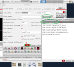
Virtuoso_ADE_Model_Library_Setup.png

You can see the parasitic caps and its values when you open the extracted view.

There exists also the possibility to backannotate the parasitics into the layout view (AFAIR), where they are much simpler to be found and assigned to their relative nodes.

3) Can I link the symbol to the extracted layout not the schematic?
This might be another possibility.
 
You want to use Hierarchy Editor and make a config view
for the simulation testbench schematic. For running post
layout sims you will open the config view (allowing the
schematic to open as well) and kick off the simulation
from that particular (schematic) window. In the config
view, you change the active view of the chip from
"schematic" to "analog_extracted" (or whatever the
name of the "refined" extracted netlist, so-prepared,
view is).

The connectivity (LVS) extracted netlist wants the
parasitics "massaged" (filtered, combined, etc.). There
is a menu based process for doing this. Last I looked
it was something like "refine extracted netlist" or like
that.
 
For a 0.5um technology, the parasitics of a "good" layout shouldn't decrease/increase the schematic simulation values not more than about 10%
(concerning input capacitance, propagation delay, slew rate, max. operating frequency).

how can I know my layout is good? maintaining minimum DRC spacing between layers for example?


As you've successfully extracted your layout, there should an extracted view and an extracted netlist be available, both already containing the parasitics.

Actually, when the Extractor window pop-up, I set the 'Set Switches' to 'Extract_parasatic_caps' and then I did extraction and the parasitic caps appear in the extracted layout. It means now I don't need to do QRC, Am I right?

In the ADE Setup --> Design ..., select the extracted view,

I followed these steps but the simulation did not start and I can not probe any voltage or current in my schematic, Is there any reason making this problem?


This might be another possibility.

would you please advise how can I make a symbol using my extracted layout? I am using a schematic/Layout view not netlist.

- - - Updated - - -

You want to use Hierarchy Editor and make a config view
for the simulation testbench schematic. For running post
layout sims you will open the config view (allowing the
schematic to open as well) and kick off the simulation
from that particular (schematic) window. In the config
view, you change the active view of the chip from
"schematic" to "analog_extracted" (or whatever the
name of the "refined" extracted netlist, so-prepared,
view is).

The connectivity (LVS) extracted netlist wants the
parasitics "massaged" (filtered, combined, etc.). There
is a menu based process for doing this. Last I looked
it was something like "refine extracted netlist" or like
that.

would you please elaborate more on using Hierarchy Editor ?
 

File>New, same cellname as your simulation testbench,
type="config". Base view = schematic. This opens a
table-looking view and another window of your testbench.

Edit the switch-view and stop-view lists to match your
way of working. Update the views. In the config table
each master should now show which view type it's using.
You can alter this "surgically" (e.g. change the view of
the design-under-test, that sits in the testbench, from
"schematic" to "analog_extracted", so you are running
from the extracted view w/ refined parasitics).

When you change the view switching, then force a
re-evaluation (as lower hierarchy may be traversed in
a very different way). You can save the preferred
hierarchy (config view) and not have to re-jigger the
netlisting every time you come back to it.

At some later time you will File>Open the config view,
with schematic as well (check box), to simulate with
arbitrary configuration (re specific hierarchy for each
element) as you have been doing from schematic,
fixed view-switching (from master switch/stop list).

From the spawned schematic bound to the Hierarchy
Editor session, kick off your simulation in the usual
way.

You can also, I'm told, change specific individual
instances' switch/stop rather than all instances of
same master. But I never exercised this mode, before
stepping away from Cadence.
 
how can I know my layout is good? maintaining minimum DRC spacing between layers for example?
Right, concerning small parasitics (low propagation delay or high operating frequency).
And short routing connections, especially for time-critical paths.


... the parasitic caps appear in the extracted layout. It means now I don't need to do QRC, Am I right?
Yes!


I followed these steps but the simulation did not start and I can not probe any voltage or current in my schematic, Is there any reason making this problem?
I think the simulator neither found the (analog-)extracted view, nor the extracted netlist.


would you please advise how can I make a symbol using my extracted layout? I am using a schematic/Layout view not netlist.
This has already been answered by dick_freebird above, I guess.
 
File>New, same cellname as your simulation testbench,
type="config". Base view = schematic. This opens a
table-looking view and another window of your testbench.

Edit the switch-view and stop-view lists to match your
way of working. Update the views. In the config table
each master should now show which view type it's using.
You can alter this "surgically" (e.g. change the view of
the design-under-test, that sits in the testbench, from
"schematic" to "analog_extracted", so you are running
from the extracted view w/ refined parasitics).

When you change the view switching, then force a
re-evaluation (as lower hierarchy may be traversed in
a very different way). You can save the preferred
hierarchy (config view) and not have to re-jigger the
netlisting every time you come back to it.

At some later time you will File>Open the config view,
with schematic as well (check box), to simulate with
arbitrary configuration (re specific hierarchy for each
element) as you have been doing from schematic,
fixed view-switching (from master switch/stop list).

From the spawned schematic bound to the Hierarchy
Editor session, kick off your simulation in the usual
way.

You can also, I'm told, change specific individual
instances' switch/stop rather than all instances of
same master. But I never exercised this mode, before
stepping away from Cadence.

Thank you so much dick_freebird, I can now simulate both Sch and extracted with parasitics at the sametime. It is really super easy with using Config than older way of modifying the settings from ADE opened from Layout-extracted view. Anyway, I want to share with you also this helpful video I found on youtube for those who are interested, unfortunately it's a silent video :) but it does the job bsides dick_freebird description. https://www.youtube.com/watch?v=44xN6UHaMys


I got one concern if you could help me understanding it, does the extracted view usually include also parasitic resistances if any? or only stray caps? if it does show all, in my extracted layout I only see caps?
 

C-only extract I think is the default, simplest, oldest
and bothers the netlist only by addition of a whole lot of
shunt C elements.

RC extract actually has to break the netlist to insert
series R and these tools are newer, "bloatier" and have
to be invoked specifically.

By newer I mean a decade old instead of 3....

Is there a way or specific setting modifications to do an RC extract? or this is usually done with help of other extra tools something like QRC ..etc?
 

If you have C extraction in your extracted view, it means you are already using one of the extraction tools, possibly unknowingly.
Extraction mode - C, RC, R, or device-only - is one of the typical input settings to extraction tool, either in extraction tool command file, or in extraction tool GUI that you bring up from Virtuoso.
What is the default mode, that depends on local design flow settings.

There are many more settings in parasitic extraction (a few hundred commands, in each extraction tool), that significantly affects the results, such as accuracy, post-layout netlist size, etc. - for example, parasitic reduction settings, whether or not to extract power nets, via merging, etc. etc.
 

If you have C extraction in your extracted view, it means you are already using one of the extraction tools, possibly unknowingly.
Extraction mode - C, RC, R, or device-only - is one of the typical input settings to extraction tool, either in extraction tool command file, or in extraction tool GUI that you bring up from Virtuoso.
What is the default mode, that depends on local design flow settings.

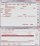
It seems that I have Diva tool, and usually I do extraction in three steps as shown in the attached file, (1) set switches (2)parasatic_caps (3)ok.
 

Attachments

  • Untitled.png
    Untitled.png
    288.1 KB · Views: 285

Status
Not open for further replies.

Part and Inventory Search

Welcome to EDABoard.com

Sponsor

Back
Top