Continue to Site

Welcome to EDAboard.com

Welcome to our site! EDAboard.com is an international Electronics Discussion Forum focused on EDA software, circuits, schematics, books, theory, papers, asic, pld, 8051, DSP, Network, RF, Analog Design, PCB, Service Manuals... and a whole lot more! To participate you need to register. Registration is free. Click here to register now.

Determine Technology Current using foundry models

Status
Not open for further replies.
With such an extremely simple circuit (and my models)
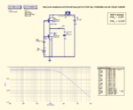
simple_inverter-amp.png ... i got 35dB gain and a UGB≈200MHz - if you don't mind the high current of 1.7mA .

Note: such a circuit is just good for simulation, it's not appropriate for real analog amp design (uncontrolled drain current, high sensitivity on Vth and W/L ratio values, and PVT changes).

For higher gain and lower power consumption better use the differential amplifier version (OTA), s. my example above.
 
Sir,
I repeated the procedure for PMOS to find the technology current.

Again, the values obtained are over a wide range.

for W/L = 1
IC = 0.01 Id = 4.519nA =>Io = 452nA
IC = 0.48 Id = 83.57nA =>Io = 174nA
IC = 10 Id = 1.54uA => Io = 154nA

Hence, I have opted for Iop = 300nA
 

I have opted for Iop = 300nA

I recommend to not ascertain a fix value to Io, but take that one which you obtained for an Id value (for W/L=1), accordingly IC, - similar to that Id you want to operate the transistor with. With that value calculate your W/L ratio(s).
 

I recommend to not ascertain a fix value to Io, but take that one which you obtained for an Id value (for W/L=1), accordingly IC, - similar to that Id you want to operate the transistor with. With that value calculate your W/L ratio(s).

Sir,

I do realize that there should not be much dependence on value of Io.

Kindly comment on issues in ota design example

- - - Updated - - -

Try something like this:
View attachment 140998[/QUOTE]

I am facing issues with regards to key step in the design:

from gm vs IC , I obtained IC at gm= 62uS.


Please clear this
1.Using Id,I0, L and IC , value of W is determined. ( as in the book)
In the above design , what did you fix first for differential pair
OR
2. keep W / L = 1 and plot gm vs IC
For gm = 62.7uS find IC.

I have referred the book but still no clarity.
 

I simply took the I0 value which you decided to choose: ... assumed 1/3 of this value for pMOS-I0, then estimated/calculated the necessary W/L ratios to achieve the required UGB for your C0;
gm & gain values were the results.


Sir,

I have designed the differential amplifier (with current mirror load) with

Iss = 4uA

Fixed input and output CM level to 900mV

M1,2 vth = 497m
vgs1,2 = 545m

normalized voltage, v = 0.69
IC from formula = 1.19

Design Choices of IC

Amplifying Transistors IC = 0.942.
Tail current source IC =4.217
current mirror load IC = 25.25


differntialamp_withCurrentmirror.jpgdifferntialamp_withCurrentmirror.jpgdifferential_amplifier.jpg

Gain = 45 dB
UGB = 550 kHz
gm = 34uA/V2


I need to increase the current in order to get more gm.

However, I still don't feel confident about this technique.

My concern is that amplifying transistors can be designed for certain current or gm.
 

Iss = 4uA

Fixed input and output CM level to 900mV

M1,2 vth = 497m
vgs1,2 = 545m

normalized voltage, v = 0.69
???
IC from formula = 1.19

Design Choices of IC

Amplifying Transistors IC = 0.942.
Tail current source IC = 4.217
current mirror load IC = 25.25

Gain = 45 dB
UGB = 550 kHz
gm = 34uA/V


Amplifying Transistors IC = 0.942 : you chose moderate inversion, ok
Tail current source IC = 4.217 : strong inversion, ok for current source
current mirror load IC =25.25 : absolutely wrong, this ruins all the gain from your Amplifying Transistors !


Didn't you study my above example? Your current mirror load pair should operate in a similar inversion mode like your amplifying transistors. Operating in (very) strong inversion mode ruins your gain.

Note the different I0 for PMOSFETs.

I need to increase the current in order to get more gm.

I don't think so.

BTW: Does your ac voltage source include a DC voltage source (same as at the other diff. input)?


Amplifying Transistors IC = 0.942 : you chose moderate inversion, ok
Tail current source IC = 4.217 : strong inversion, ok for current source
current mirror load IC =25.25 : absolutely wrong, this ruins all the gain from your Amplifying Transistors !


v = normalised overdrive voltage .
After choosing the IC , calculated the normalized voltage,v using the plot between IC and v .
v = 0.69
Vov = v * 2*n * Vt = 0.69*0.07 =0.0483
Vgs = Vth + Vov = 0.545

v = (overdrive voltage Vov )/(2*n*Vt)
Vt: thermal voltage
n = 1.4


From v => Vgs was determined.
Since input common mode level is fixed, I chose the source potential to ensure required Vgs is obtained.
In this case:
Vg= 900mV
Vth = 497mV

Vgs = 545mV and Vg = 900mV
Vs = 355mV (Vds for tail current source)

The common mode level is 900mV. For current 2uA and I0p = 300nA , I obtained this value of IC.

As told by you earlier, the value of Io can't be fixed.

I don't understand how output resistance of PMOS current source (and hence gain) is controlled by W.


Didn't you study my above example? Your current mirror load pair should operate in a similar inversion mode like your amplifying transistors. Operating in (very) strong inversion mode ruins your gain.

Note the different I0 for PMOSFETs.


I don't think so.

BTW: Does your ac voltage source include a DC voltage source (same as at the other diff. input)?
Yes, it does. 900mV DC
 
Last edited:

I don't understand how output resistance of PMOS current source (and hence gain) is controlled by W.

Not by W (alone). W/L, respectively the inversion mode is the reason.

Remember the gm/Id vs. IC curve?
gmoverId_vs_IC.png
 
Not by W (alone). W/L, respectively the inversion mode is the reason.

Remember the gm/Id vs. IC curve?
View attachment 141370

for load transistors, I kept required voltages at the transistors and chose the W for current.

Because the technology current 300nA in PMOS,
IC = 1uA/(0.3u * W/L)
W = 0.264u L = 1u
IC = 25.25
 

If I fix the current, say 2uA in this case.
The terminal voltages for PMOS
Vg = Vd = 900mV (common mode output voltage)
Vs = 1.8V
Id = 2uA

Now only (W/L) ratio is the choice.
for L =1u I got W= 0.264u.
I can opt for higher L to get more gain, while keeping the W/L ratio constant.

However, IC will remain same!
 

The terminal voltages for PMOS
Vg = Vd = 900mV (common mode output voltage)
Vs = 1.8V
Id = 2uA

I forgot that you need Vg = Vd = 900mV (common mode output voltage), sorry.

And now it seems you need a PMOS input stage. Try something like this: 180nm-1stage-p-OTA-10MHz-1pF-OCMV=0.9V.sch.png
 

I need to make an NMOS input amplifier.
Going for Folded Cascode to get more swing .
 

Hi both,

Just to clarify, one of you said that we need several I0 current?

Is this correct? Do you need several I0 currents?
 

I forgot that you need Vg = Vd = 900mV (common mode output voltage), sorry.

And now it seems you need a PMOS input stage. Try something like this: View attachment 141857

I need to design cascode diff amplifer and folded cascode diff amp
But, there are doubts regarding the setup

In differential amplifier,
Output and Input common mode level was fixed.
so, the set-up was quite simple .
Vd =900mV
Vg = 900mV

I kept tail current source in strong inversion and used IC = 10


In Cascode diff amp , gate voltage at diff pair is known ( input CM level = 900mV)
But, because of the cascode transistor , I am not sure about drain voltage of input pair.

Design specs,
GBW = 1MHz Cl = 10pF
gm = 62.6uA/V
What set-up should be used to determine gmbyid for M1-M2 pair ?

- - - Updated - - -

I need to design cascode diff amplifer and folded cascode diff amp
But, there are doubts regarding the setup

In differential amplifier,
Output and Input common mode level was fixed.
so, the set-up was quite simple .
Vd =900mV
Vg = 900mV

I had kept tail current source in strong inversion and used IC = 10


In Cascode diff amp , gate voltage at diff pair is known ( input CM level = 900mV)
But, because of the cascode transistor , I am not sure about drain voltage of input pair.

Design specs,
GBW = 1MHz Cl = 10pF
gm = 62.6uA/V
What set-up should be used to determine gmbyid for M1-M2 pair ?

Is this setup correct?
gmoverid_by_ID.jpg


To begin with, I used a sweep of voltage source at the drain terminal

I had kept W as variable.

Plotted
1. gmoverid vs IC
2. id vs IC

For IC = 1.31579
gm/Id = 17.35 and Id = 3.8uA

From this,
Id is chosen as 3.8uA.
gm obtained is 65uA

gmoverid_vs_IC_2.jpg


But,
how to calculate W?
 

INVERSION COEFFICIENT BASED DIFF AMP

TAIL CURRENT SOURCE ISS = 20 uA
Wtail = 13
W1/L1 = 1
Gm = 64.77u
Gmoverid = 6.73
Vdsat = 252m
Rout = 3.075M
Vth = 455.127 mV
IC = 9.8/0.95

PMOS
WP1 = 1.76u
IC = 18.94


RESULTS
GAIN = 39.64dB
UGB = 1MHz

However, I expect CMRR to be low due to very large transistor as the tail current source
 

Status
Not open for further replies.

Part and Inventory Search

Welcome to EDABoard.com

Sponsor

Back
Top