Continue to Site

Welcome to EDAboard.com

Welcome to our site! EDAboard.com is an international Electronics Discussion Forum focused on EDA software, circuits, schematics, books, theory, papers, asic, pld, 8051, DSP, Network, RF, Analog Design, PCB, Service Manuals... and a whole lot more! To participate you need to register. Registration is free. Click here to register now.

Produce pulse of +28VDC

Status
Not open for further replies.

TXRX

Full Member level 2
Joined
Mar 7, 2012
Messages
143
Helped
2
Reputation
4
Reaction score
5
Trophy points
1,298
Activity points
2,252
Hi,

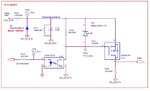
I attached, I design a circuit that produce pulse of maximum of +28VDC at the output from a uC that produce pulse of +3.3VDC, I put a zener of +9.1V that will protect Gate to Source of the FET from over voltage but it is limit the output volage to the zener voltage , How can improve the curcuit ?

Thanks,

Doron
 

Attachments

  • Pulse Circuit.jpg
    Pulse Circuit.jpg
    227.2 KB · Views: 71

Insert a resistor between the optocoupler output and the zener anode. The MOSFET output will then be able to go up to 28V, but the pulse rise time will be somewhat slower due to the gate charge.

In the present circuit, the output voltage is limited to the zener voltage because the optocoupler output is connected directly to the zener anode. When you have a pulse and the opto output transistor saturates, it pulls the zener anode to approximately 0V. That pulls down the cathode to about 9V and that's also the MOSFET supply voltage.

If you insert the resistor as suggested, the zener anode will no longer be pulled down to 0. The difference voltage of approximately 19V will be absorbed by the new resistor.
 

Inserting a resistor between optocoupler output and zener diode will never turn on mosfet as this will create voltage divider at gate of mosffet. Mosfet gate should go to low voltage for turn on.Instead changing zener diode position from gate to drain will protect gate during Mosfet off condition.and at on codition mosfet gate will directly connect to ISO_DC_RTN,this will turn on mosfet.
 

Inserting a resistor between optocoupler output and zener diode will never turn on mosfet as this will create voltage divider at gate of mosffet. Mosfet gate should go to low voltage for turn on.Instead changing zener diode position from gate to drain will protect gate during Mosfet off condition.and at on codition mosfet gate will directly connect to ISO_DC_RTN,this will turn on mosfet.
Look at the modified circuit I've attached and note the voltages circled in RED when the optocoupler is in the ON state. The MOSFET gate voltage is still 9.1V below the source voltage. that is, Vgs = -9.1V. This will certainly turn the MOSFET on. But the source is now maintained at 28V, therefore the drain voltage can now pull up to 28V.

To make it clearer, I've also added the current distribution in GREEN colour.

As I said before, since the additional resistor is in series between the opto and the gate, this will increase the rise time of the gate drive. This may or may not matter depending on the intended application. Using a lower power P MOSFET with lower gate charge and capacitance (like say a BSS84) will reduce that effect.

Modified circuit.png
 

Inserting a resistor between optocoupler output and zener diode will never turn on mosfet as this will create voltage divider at gate of mosffet. Mosfet gate should go to low voltage for turn on.Instead changing zener diode position from gate to drain will protect gate during Mosfet off condition.and at on codition mosfet gate will directly connect to ISO_DC_RTN,this will turn on mosfet.

Why will the mosfet not turn on ? :

VGS will be: -9.1VDC and the Max VGS of the MOSFET is -3VDC, so where is the problem ?
 

Status
Not open for further replies.

Similar threads

Part and Inventory Search

Welcome to EDABoard.com

Sponsor

Back
Top