Continue to Site

Welcome to EDAboard.com

Welcome to our site! EDAboard.com is an international Electronics Discussion Forum focused on EDA software, circuits, schematics, books, theory, papers, asic, pld, 8051, DSP, Network, RF, Analog Design, PCB, Service Manuals... and a whole lot more! To participate you need to register. Registration is free. Click here to register now.

Why is the thermal pad of this power IC not made bigger than 3mm x 3mm?

Status
Not open for further replies.
T

treez

Guest
Hello
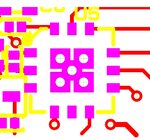
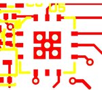
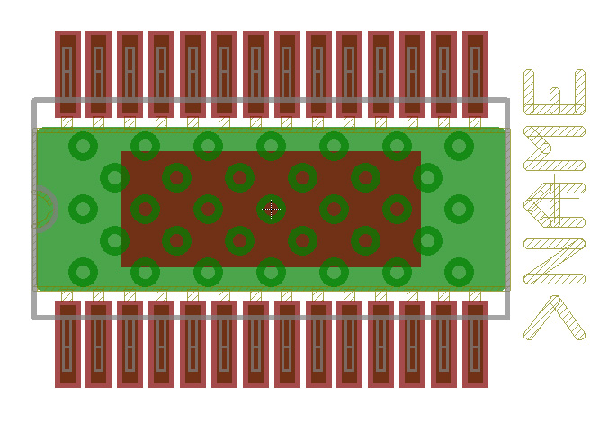
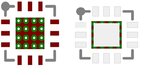
The 25th page of the below app note shows the land pattern of an offline linear LED driver IC.
The FETs in this package operate in the linear region.
Why is the land pattern showing a central thermal pad of dimension just 3mm by 3mm?
There is room there to make it 4mm by 4mm and still have plenty of clearance away from the actual outer pads. The solder mask could still be 3mm by 3mm so that the IC “locates” in the centre of the land pattern during the reflow soldering process.
So why have the manufacturers not recommended a bigger thermal pad for this IC?

DT3001 LED driver IC
http://www.seoulsemicon.com/_upload/Goods_Spec/Acrich2-Applicationnote.pdf
 

Hi,

My assumption:
It has to do with die size.

Klaus
 

Thanks,
I think we can make the chip run cooler if we make the centre thermal pad 4mm by 4mm (and use a 3mm by 3mm solder mask so it locates centrally in the reflow machine).
D'you think its a good idea?
 

You can certainly make the thermal pad larger, provided it doesn't interfer with the outer pads. Just be sure to mask the extra, like you said, so that the part doesn't float on the extra solder.
 
  • Like
Reactions: treez

    T

    Points: 2
    Helpful Answer Positive Rating
Thanks, the 4x4 pad is more than 50% biger then the 3x3 pad so we will be able to get more thermal vias in it, and much better cooling.....i wonder why Seoul Semiconductor did not say a 4x4 thermal pad was allowable?
I mean surely making it 4x4 is a win/win situation?

- - - Updated - - -

Our PCB layout engineer has placed five thermal vias of diameter 0.65mm in the thermal pad of our DT3001 IC. (as in the jpeg attached).
he seems to have just used five square PTH vias, which as you can see , dont fit together very well and hence there is solder resist between them. Is this bad?
So he has got solder resist over the thermal pad. (as attached)
Surely 0.65mm is way too big for a thermal via in such a small thermal pad?
(he has made the thermal pad 3mm x 3mm)
 

Attachments

  • Solder resist in thermal pad of DT3001 IC.jpg
    Solder resist in thermal pad of DT3001 IC.jpg
    65.4 KB · Views: 186
  • Thermal vias in pad of DT3001 IC.jpg
    Thermal vias in pad of DT3001 IC.jpg
    63.8 KB · Views: 151
Last edited by a moderator:

The whole center of the footprint should be one solid pad. 0.65mm is way too large for the vias - all of the solder will go down the holes. Use something like 0.3mm and add a bunch more. Absolutely NO solder mask in the 3x3 center region.

I was going to add a picture of one of my power devices with a center pad, but apparently I can no longer do that.
 
  • Like
Reactions: treez

    T

    Points: 2
    Helpful Answer Positive Rating
Thanks, I agree with you but our PCB contractor has convinced the company that the thermal pad construction of post #5 is correct. He has declared that he got this OK’d with a PCB assembly company. He says that the solder resist that exists in the thermal pad is needed to stop the solder going down the five 0.65mm diameter vias.
To me , it just looks like he’s slapped in five through hole vias to kind of make up the thermal pad.
 

Thanks, I agree with you but our PCB contractor has convinced the company that the thermal pad construction of post #5 is correct.

Well, convince him that you control the board and you don't want to do it that way. Who's going to have to fix the board when it doesn't work properly, your PCB contractor, or you? They are just taking the easy way out. Tell them to $uck it up and just do what they are told.

The 0.65mm vias are way too large, IMO. They should be less than half that size and with a whole lot more. Here's an image of a pad with holes in the pad. As for solder, you should expect solder to go down the holes, so the volume should be adjusted accordingly.

The vias in the image are 0.012" in diameter (~ 0.30mm).

 
  • Like
Reactions: treez

    T

    Points: 2
    Helpful Answer Positive Rating
If the vias are not to be filled (like, solder masked PTH)
then all thermal conduction is by the sidewalls and you
do not benefit from via area but rather via periphery.
It might be that you would be well better off with more,
smaller vias. This ought to be a simple Excel what-if, if
you have the PCB groundrules and via construction info
handy.

Of course controlled solder filling would be superior in
terms of vertical thermal conduction. But "controlled"
may be hard to come by. Is there a solid core thermal
via? Or ones with thicker walls than the high density
electrical vias?
 
  • Like
Reactions: treez

    T

    Points: 2
    Helpful Answer Positive Rating
That pad is wrong... maybe your PCB contracter should be sacked, especially if he is the one to use oversized switching nodes on SMPS's.
I would suggest you buy IPC-7093 and make him read it...
0.3mm thermal via size, most common size used on thousands of designs....
 
  • Like
Reactions: treez

    T

    Points: 2
    Helpful Answer Positive Rating
Thanks, we changed the thermal pad footprint to the attached.
We used a 3.5mm x 3.5mm copper square, and put 0.3mm thermal vias as near as possible 1mm apart. (centre of drill to centre of drill)
The right hand image’s “whited out” bits are where there is no solder resist.

- - - Updated - - -

We hope that the sixteen 0.3mm thermal vias won't wick away too much of the solder paste during the reflow process?
 

Attachments

  • Thermal pad of Power IC.jpg
    Thermal pad of Power IC.jpg
    24.6 KB · Views: 178

I don't think you need that many thermal vias, the aim is to have a basic 50-70% of the pad soldered and void free, higher is better.
 
  • Like
Reactions: treez

    T

    Points: 2
    Helpful Answer Positive Rating
Thanks,
the thermal pad is 3.5mm by 3.5mm
Each of the 16 drills is 0.3mm in diameter.

As such, only 9.2% of the pad area is holes.

So do you think we will be OK with this?
 

Its too many, the data sheet will cover the thermal aspects of the device, read that. For a device that size I would use between 5 and absolute max 12 depending on the thermal requirements of the circuit.
 
  • Like
Reactions: treez

    T

    Points: 2
    Helpful Answer Positive Rating
Also to do it for best effect, having the vias filled with conductive epoxy will best transfer the heat to the other copper layers rather than use the extremely thin plated walls.
That way you can also have less vias as you would have more heat transfer through them.

Although this adds cost to the board, hence why a lot do not use it.
 
  • Like
Reactions: treez

    T

    Points: 2
    Helpful Answer Positive Rating
Thanks, i suppose if we use conductive epoxy in the vias, then it will not matter that there are so many of them, because the solder will not wick away down them when they are filled with conductive epoxy?

- - - Updated - - -

For a device that size I would use between 5 and absolute max 12 depending on the thermal requirements of the circuit.
Thanks, we have an array of 16 thermal vias which are 0.3mm diameter and the drill centres are 1mm apart…I thought this was the standard minimum allowable spacing for thermal vias?

- - - Updated - - -

We actually oversized the pad by 36%, so I think we can be granted the 16 holes?
(Our thermal pad is 3.5mm by 3.5mm unlike the datasheet one which is just 3mm by 3mm)
 

I'm of the opinion that your 16 holes are just fine. However, ask your manufacturing engineer if he concurs. In the ApNote, it appears that they do not use any vias through the board. This would explain why the Θjc and the θjb have such wide differences (and the case is better than the board). This device will dissipate a lot of heat, so you must find a way to manage this heat and rout it away from the device. The ApNote says that the thermal pad "must not be connected to any electrical node", which means that it must be an orphan and not even connected to ground.

Tell us what the power dissipation for the device will be in your circuit design.
 
  • Like
Reactions: treez

    T

    Points: 2
    Helpful Answer Positive Rating
Status
Not open for further replies.

Part and Inventory Search

Welcome to EDABoard.com

Sponsor

Back
Top