Continue to Site

Welcome to EDAboard.com

Welcome to our site! EDAboard.com is an international Electronics Discussion Forum focused on EDA software, circuits, schematics, books, theory, papers, asic, pld, 8051, DSP, Network, RF, Analog Design, PCB, Service Manuals... and a whole lot more! To participate you need to register. Registration is free. Click here to register now.

Cadence Custom Layout for beginners -RF IC design

Status
Not open for further replies.
R

rty94

Guest
It's the first time that I am creating a layout for an LNA design at 35Ghz. What should I read or watch for understanding how to create the layout, metals, how to use the rules of the manual etc?


Thanks!
 

You should pay attention to many things but as Bahzad Razavi said in a training..
Symmetry,Symmetry,Symetry...Decoupling,Decoupling,Decoupling...It's just a motto but this is absolutely true.

35GHz is really high frequency and I recommend you to read and study previous various papers of other authors to be "inspired". Otherwise there isn't any "plug-and-play" rules for drawing of a layout.
 

There are lots of issues in IC layout and you have to consider them.So it is hard to explain all of them. but important ones can be

1) If you are designing differential LNA symmetry is really important. So for example you apply techniques like Common-Centriod for your transistors in order to avoid post fabrication mismatches. There are significant matching errors when using transistors, or resistors, or capacitors, if common-centroid layout isn't used. There are always more-or-less linear gradients across a die.

2) In high frequencies even a short connection between two blocks can be a parasitic (jLw) so you have to minimize them as much as you can.

3) EM simulation MUST be done in order to optimize circuit. You will observe parasitic effects (like inductor and capacitor self resonance and parasitic resistances) and also Coupling between two inductors.

So for example if two transistors are close to each other and effecting each other, you may rotate one (Probably you will have lines not inductors with turns, since your frequency is high)

4) You have to do power distribution. It means that you cannot connect one component from only one corner or part to another one and you should distribute your signal.

and many other things ...


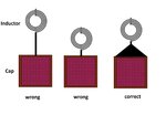
layout.jpg
 

Status
Not open for further replies.

Part and Inventory Search

Welcome to EDABoard.com

Sponsor

Back
Top