CAMALEAO
Full Member level 4
Hi everyone,
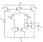
I have a question regarding a two stage opamp in which I can't visualise/imagine in an intuitive way but I see everybody saying the same thing leading me to wonder if those people know really why.
What I normally hear people saying, for example, regading a two stage opamp with the miller cap for compensation is something like this: because this is a high gain node the voltage here will not vary much, the amplifier with try to maintain this voltage always constant. Say at the gate of the second stage MOSFET.
Question: Is this really true, this affirmation? I mean, you can see that it is true through simulation, but why? Can this be explained wirh words or with equations? OK, this is providing that the opamp is in negative feedback - I guess.
Regards.
