atlantis7
Member level 2
Hi
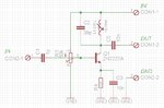
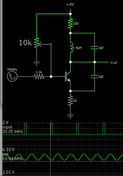
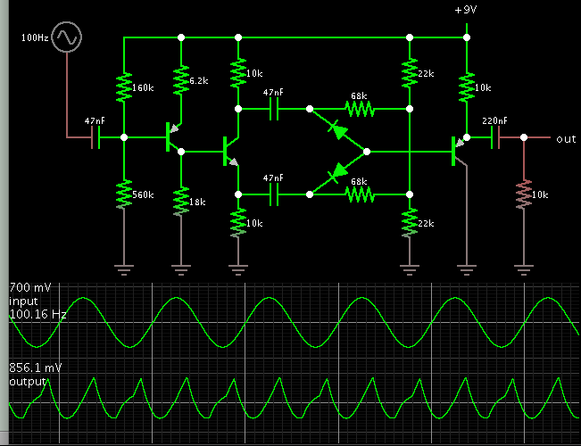
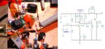
The current task I have trouble with is building a bjt frequency doubler. Unfortunately I haven't been able to find a lot of practical hands-on design information but the circuit I built seems to be considered a working one in general. If someone knows a hands-on design guide somewhere please point me to it.
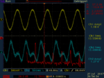
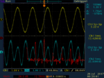
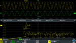
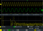
Right now the input is 13.5 MHz 1 V p-p and the output is supposed to be 27 MHz but I don't get anything usable out of it. The best I see is a distorted and much attenuated input frequency. First I had fixed resistors for the base bias whose values worked ok in a previous non-multiplier amp but when it made trouble I also tried 10k, 25k and 50k trimmers. The inductor is self-wound and should be in the right ballpark, however I also exchanged the resonant capacitor for slightly different values just to make sure. I did use a bread-and-butter 2222 transistor on purpose; although it might not be the best choice the working frequency is still way below the fT of 300 MHz.
Where's the pitfall? There must be one but I just don't see it.
Regards
Martin
The current task I have trouble with is building a bjt frequency doubler. Unfortunately I haven't been able to find a lot of practical hands-on design information but the circuit I built seems to be considered a working one in general. If someone knows a hands-on design guide somewhere please point me to it.
Right now the input is 13.5 MHz 1 V p-p and the output is supposed to be 27 MHz but I don't get anything usable out of it. The best I see is a distorted and much attenuated input frequency. First I had fixed resistors for the base bias whose values worked ok in a previous non-multiplier amp but when it made trouble I also tried 10k, 25k and 50k trimmers. The inductor is self-wound and should be in the right ballpark, however I also exchanged the resonant capacitor for slightly different values just to make sure. I did use a bread-and-butter 2222 transistor on purpose; although it might not be the best choice the working frequency is still way below the fT of 300 MHz.
Where's the pitfall? There must be one but I just don't see it.
Regards
Martin