sys_eng
Full Member level 4
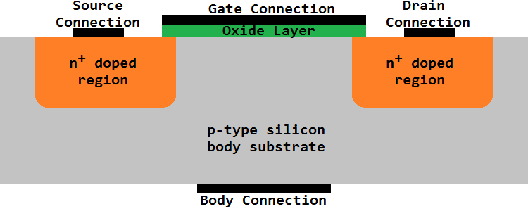
PSpice NMOS model with body tied to source

usually body should tied to ground for nmos.
why is it tied to the source? The source and body shouldnt be the same, right?
usually body should tied to ground for nmos.
why is it tied to the source? The source and body shouldnt be the same, right?