Continue to Site

Welcome to EDAboard.com

Welcome to our site! EDAboard.com is an international Electronics Discussion Forum focused on EDA software, circuits, schematics, books, theory, papers, asic, pld, 8051, DSP, Network, RF, Analog Design, PCB, Service Manuals... and a whole lot more! To participate you need to register. Registration is free. Click here to register now.

Matching of huge devices

Status
Not open for further replies.

mult

Junior Member level 1
Joined
Jan 17, 2013
Messages
18
Helped
0
Reputation
0
Reaction score
0
Trophy points
1,281
Activity points
1,442
Hi everybody!

My design uses huge devices which are high voltage devices.
The problem is that I doubt they should be matched in the same way as regular devices.
Does it really make sense to apply the same technique for matching (common centroid for example) when dimensions are so large.
Please see attached picture for reference.
case 1: common centroid layout of two HVNMOS
case 2: multi-finger structure for both devices

Could it be that the advantages of common centroid layout are offset by a significant increase of spacing between matching devices?
Which case (1 or 2) are preferable?
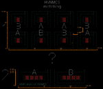
Image 6.jpg

Thanks for your opinion!
 

Could it be that the advantages of common centroid layout are offset by a significant increase of spacing between matching devices?
Yes, I think so.

Which case (1 or 2) are preferable?
I'd think: case 2: multi-finger structure for both devices is well enough.
 
  • Like
Reactions: mult

    mult

    Points: 2
    Helpful Answer Positive Rating
How high is your "high voltage"?

Why do you need to match these two devices?

It seems that "huge" size is required to make Rdson low, and to handle large currents.
Please note that while device resistance goes down with its gate width (or area), resistance of BEOL interconnects will go up, and may contribute a significant fraction to the total Rdson - so your mismatch may be caused by interconnects.
There may be other things related to interconnects - like uniformity of current distribution over the device area, current density / electromigration issues, thermo-mechanical reliability problems if these devices are used in automotive or other applications with repetitive power pulsing, etc.

Regarding your layouts - case (2) will definitely save you area, and simplify metallization routing.
 
  • Like
Reactions: mult

    mult

    Points: 2
    Helpful Answer Positive Rating
The main things that a CC layout style gives you are
resistance to temperature gradients and resistance
to lithographic effects (gradients, field loading / edge
litho effects.

First question is, why and how well these two HV devices
need to match.

Second is, how much does voltage headroom contribute
to mismatch of drain current or Vgs (VTeff) and is this
indicating that you care at all, about test-condition VT
match?

If you are trying to match at high voltage and high
current (as the "huge devices" indicates) I'd look real
carefully at how the local power density matching sits.
Because this can push VT a lot more than any mismatch.
Consider the case of a simple NMOS mirror with
Vds=Vgs=0.8V on the master and Vds=5V on the slave,
running 10mA with a close-in transistor thermal impedance
of 100degC/W junction-case. You would have 0.008W in
one and 0.05W on the other, a 4 degree temp difference.
At about -3mV/degC that's 12mV mismatch right there.
Highly variable with the voltage applied to the slave FET
and carrying some uS-mS range thermal history as well.
 
  • Like
Reactions: mult

    mult

    Points: 2
    Helpful Answer Positive Rating
Hi,

Designing electronics begins with specifications.
This are values and units.

Klaus
 

Status
Not open for further replies.

Part and Inventory Search

Welcome to EDABoard.com

Sponsor

Back
Top