eanema
Member level 2
I have been doing some studying this week. I'm trying to use a 2D electrostatic field solver to calculate the even & odd mode impedance, as well as the isolated impedance, propagation velocity, etc etc.
the approach I have taken is using Agros2D (an opensource FEM package, its actually quite nice to use http://www.agros2d.org/)
I modeled a surface microstrip differential pair with the dimensions described on this page: http://www.pcdandf.com/pcdesign/index.php/magazine/10472-simulation-1512
because it has the results from 6 different commercial impedance calculators and all the field based solvers are in good agreement.
To calculate the various capacitances and inductances I did 6 different simulations, 3 with the FR4 substrate er=4.0 and three with the FR4 substrate = 1.0:
FR4 substrate = 4.0
electrode 1=1v, electrode 2=0v
electrode 1=0v, electrode 2=1v
electrode 1=1v, electrode 2=1v
FR4 substrate = 1.0
electrode 1=1v, electrode 2=0v
electrode 1=0v, electrode 2=1v
electrode 1=1v, electrode 2=1v
Because of symmetry, simulation 1 & 2 will always yield the same result
I then found the the energy stored in the dielectric material using a volume integral of the FR4 and the Air space in the model. For er=4.0 I found three energies as follows:
We1: electrode 1=1v, electrode 2=0v
We2: electrode 1=0v, electrode 2=1v
We3: electrode 1=1v, electrode 2=1v
This means that the mutual capacitance (C12) and the capacitance to ground (C10 & C20) are found by:
Cm_FR4 = We1+We2-We3
C10_FR4 = We1-We2+We3
C20_FR4 = -We1+We2+We3
This was derived from this source: www.fieldp.com/documents/mutualcapacitance.pdf
I repeat the process of calculating C12, C10 & C20 using the data from the simulations where the FR4 was replaced with air (er=1). This is done because the magnetic field is not disrupted by FR4, it has a relative permeability of ur=1 and the inductances will be found using this field solution.
Cm_Air = We1+We2-We3
C10_Air = We1-We2+We3
C20_Air = -We1+We2+We3
Next step is to calculate the effective capacitance as per section 4.3.1 of "Advanced Signal Integrity for High-Speed Digital Designs" (hampoo.net/bbs/getattachfile/456)
For Odd mode:
Ceff_FR4 = C10_FR4 + 2*C12_FR4
Ceff_Air = C10_Air + 2*C12_Air
And Leff = 1/(2.998e8[m/s]^2 * Ceff_Air)
then Z0,odd = sqrt(Leff/Ceff_FR4)
This process is repeated for the Z0,even:
Ceff_FR4 = C10_FR4
Ceff_Air = C10_Air
And Leff = 1/(2.998e8[m/s]^2 * Ceff_Air)
then Z0,odd = sqrt(Leff/Ceff_FR4)
And also for Z0,isolated:
Ceff_FR4 = C10_FR4 + C12_FR4
Ceff_Air = C10_Air + C12_Air
And Leff = 1/(2.998e8[m/s]^2 * Ceff_Air)
then Z0,odd = sqrt(Leff/Ceff_FR4)
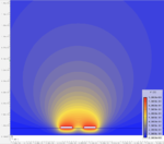
Wow, if your still reading, thank you! haha, that was a long story. Anyways, that what I'm currently doing and I'm seeing results that are very similar to the reference webpage above. The problem is that since I don't have the software packages myself, I can't be sure I'm interpreting the information that is given correctly. The page says in this image:
http://www.pcdandf.com/pcdesign/images/stories/ArticleImages/1512/bogatin3top.jpg
52.3 < Z0 < 52.9
48.8 < Zodd < 49.5
55.8 < Zeven <56.5
but my simulations, no mater what I try - increasing polynomial order, increasing mesh size, adaptive solutions based on minimum energy etc - my result is always just a little off.
I am getting:
Z0 ~= 52.3
Zodd ~= 47.7
Zeven ~= 58.0
Z0 has good agreement, but Zeven and Zodd are off.
My question to anyone who has read this far:
Do you have any suggestions as to why my calculations might be off like this? Or any ideas what I might try in order to improve the results?
Thanks to everyone who read this far!
the approach I have taken is using Agros2D (an opensource FEM package, its actually quite nice to use http://www.agros2d.org/)
I modeled a surface microstrip differential pair with the dimensions described on this page: http://www.pcdandf.com/pcdesign/index.php/magazine/10472-simulation-1512
because it has the results from 6 different commercial impedance calculators and all the field based solvers are in good agreement.
To calculate the various capacitances and inductances I did 6 different simulations, 3 with the FR4 substrate er=4.0 and three with the FR4 substrate = 1.0:
FR4 substrate = 4.0
electrode 1=1v, electrode 2=0v
electrode 1=0v, electrode 2=1v
electrode 1=1v, electrode 2=1v
FR4 substrate = 1.0
electrode 1=1v, electrode 2=0v
electrode 1=0v, electrode 2=1v
electrode 1=1v, electrode 2=1v
Because of symmetry, simulation 1 & 2 will always yield the same result
I then found the the energy stored in the dielectric material using a volume integral of the FR4 and the Air space in the model. For er=4.0 I found three energies as follows:
We1: electrode 1=1v, electrode 2=0v
We2: electrode 1=0v, electrode 2=1v
We3: electrode 1=1v, electrode 2=1v
This means that the mutual capacitance (C12) and the capacitance to ground (C10 & C20) are found by:
Cm_FR4 = We1+We2-We3
C10_FR4 = We1-We2+We3
C20_FR4 = -We1+We2+We3
This was derived from this source: www.fieldp.com/documents/mutualcapacitance.pdf
I repeat the process of calculating C12, C10 & C20 using the data from the simulations where the FR4 was replaced with air (er=1). This is done because the magnetic field is not disrupted by FR4, it has a relative permeability of ur=1 and the inductances will be found using this field solution.
Cm_Air = We1+We2-We3
C10_Air = We1-We2+We3
C20_Air = -We1+We2+We3
Next step is to calculate the effective capacitance as per section 4.3.1 of "Advanced Signal Integrity for High-Speed Digital Designs" (hampoo.net/bbs/getattachfile/456)
For Odd mode:
Ceff_FR4 = C10_FR4 + 2*C12_FR4
Ceff_Air = C10_Air + 2*C12_Air
And Leff = 1/(2.998e8[m/s]^2 * Ceff_Air)
then Z0,odd = sqrt(Leff/Ceff_FR4)
This process is repeated for the Z0,even:
Ceff_FR4 = C10_FR4
Ceff_Air = C10_Air
And Leff = 1/(2.998e8[m/s]^2 * Ceff_Air)
then Z0,odd = sqrt(Leff/Ceff_FR4)
And also for Z0,isolated:
Ceff_FR4 = C10_FR4 + C12_FR4
Ceff_Air = C10_Air + C12_Air
And Leff = 1/(2.998e8[m/s]^2 * Ceff_Air)
then Z0,odd = sqrt(Leff/Ceff_FR4)
Wow, if your still reading, thank you! haha, that was a long story. Anyways, that what I'm currently doing and I'm seeing results that are very similar to the reference webpage above. The problem is that since I don't have the software packages myself, I can't be sure I'm interpreting the information that is given correctly. The page says in this image:
http://www.pcdandf.com/pcdesign/images/stories/ArticleImages/1512/bogatin3top.jpg
52.3 < Z0 < 52.9
48.8 < Zodd < 49.5
55.8 < Zeven <56.5
but my simulations, no mater what I try - increasing polynomial order, increasing mesh size, adaptive solutions based on minimum energy etc - my result is always just a little off.
I am getting:
Z0 ~= 52.3
Zodd ~= 47.7
Zeven ~= 58.0
Z0 has good agreement, but Zeven and Zodd are off.
My question to anyone who has read this far:
Do you have any suggestions as to why my calculations might be off like this? Or any ideas what I might try in order to improve the results?
Thanks to everyone who read this far!