def_rain
Newbie level 5
Hello
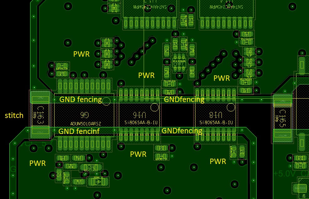
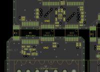
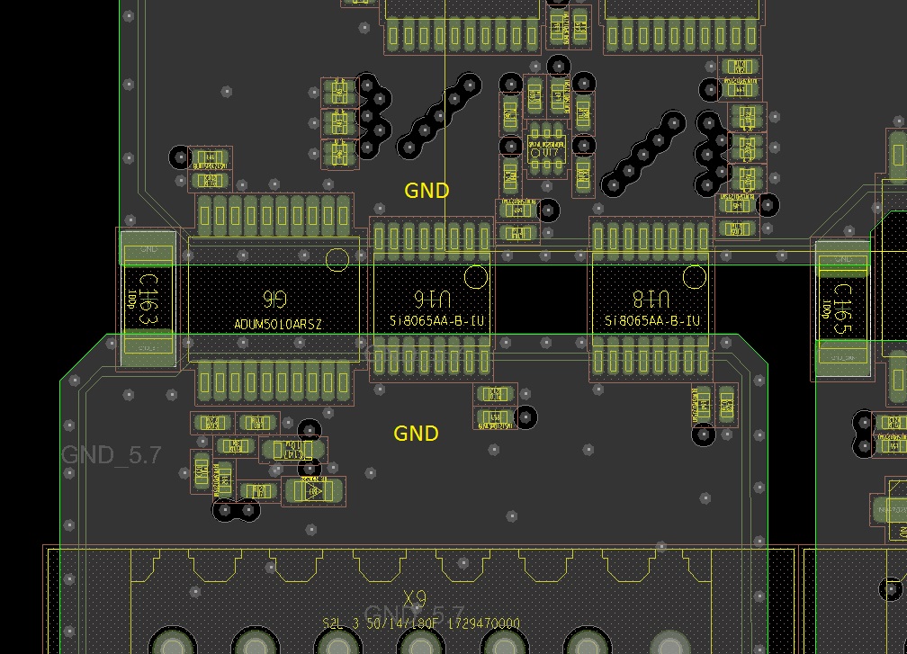
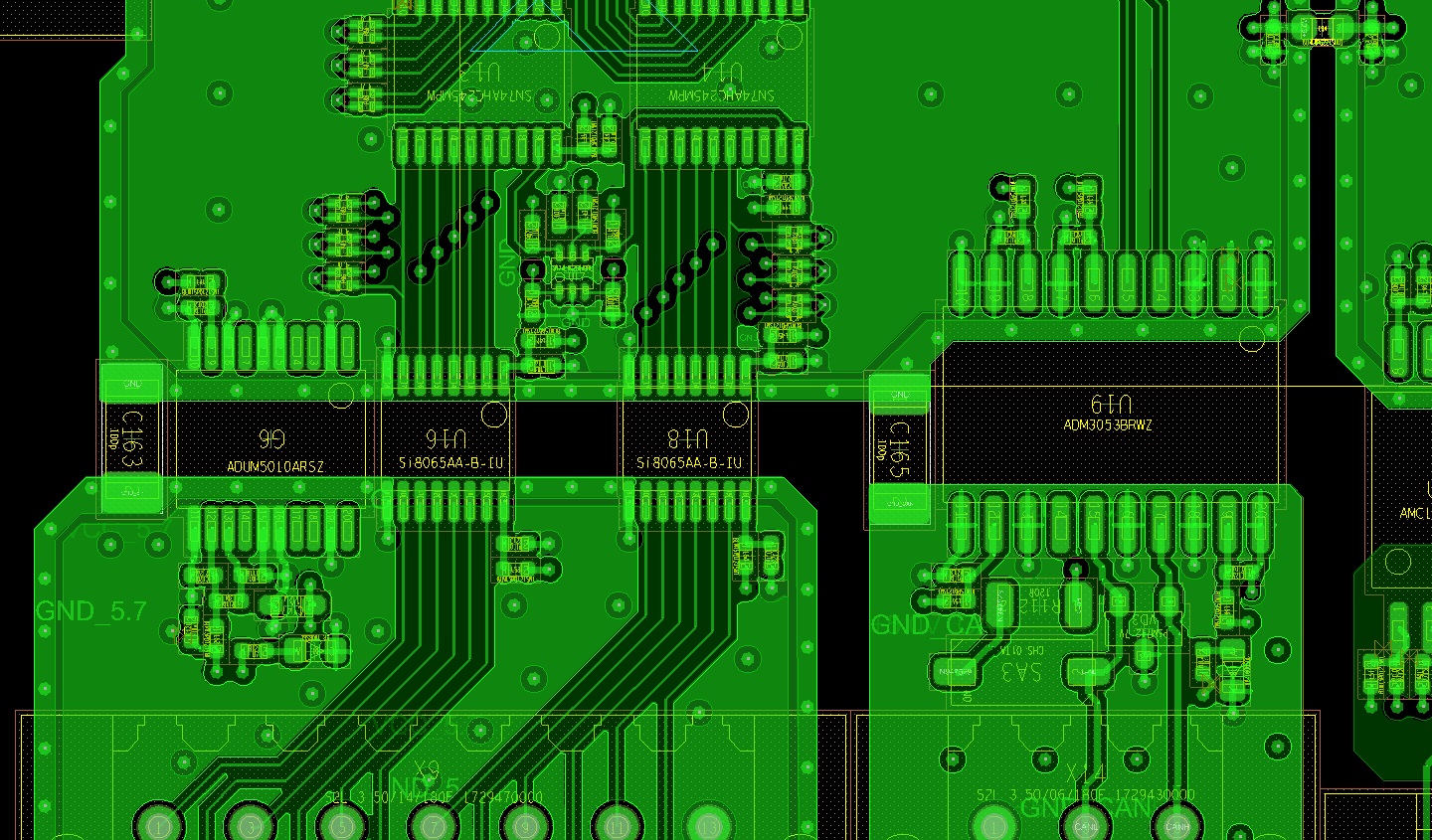
I want to apply the "Via Fence and Guard Ring" in my PCB.
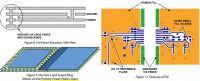
Analog Devices in its APPLICATION NOTE AN-0971 (page 9) recommends the use of a "Via Fence and Guard Ring".
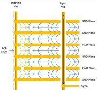
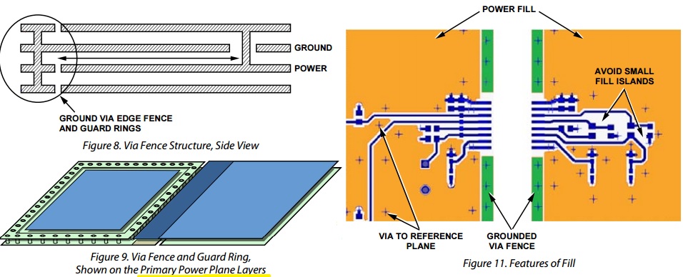
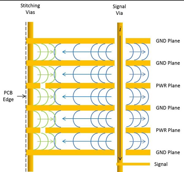
Noise on the power and ground planes that reaches the edge of a circuit board can radiate. If the edge is treated with a shielding structure, the noise is reflected back into the interplane space. This can increase thevoltage noise on the planes but reduces edge radiation.
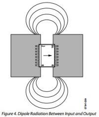
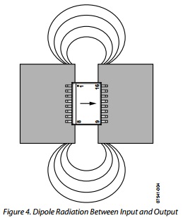
A stitching capacitor ( C163 ) between the primary and secondary side of the Digital Isolators (with isoPower inside) to reduce the Input-to-output dipole radiation.
Steck:
1 layers: TOP-GND-sign
2 layers: GND
3 layers: PWR-3.3V
4 layers: PWR-5.0V
5 layers: GND-sign
6 layers: BOT-GND
1 and 2 layers (TOP-GND-sign and PWR-3.3V)

2 layers: GND
3 layers: PWR-3.3V

I have a question: Is it possible to make a via fencing under the package of the chip in the insulating gap (as I do in the pictures)? Note that the narrowest point in the gap is the stitching capacitor.
I need your recommendations and criticism of my PCB, in which I applied these methods.
Thank you.
- - - Updated - - -
changes:
3 layers: PWR-3.3V

I want to apply the "Via Fence and Guard Ring" in my PCB.
Analog Devices in its APPLICATION NOTE AN-0971 (page 9) recommends the use of a "Via Fence and Guard Ring".
Noise on the power and ground planes that reaches the edge of a circuit board can radiate. If the edge is treated with a shielding structure, the noise is reflected back into the interplane space. This can increase thevoltage noise on the planes but reduces edge radiation.
A stitching capacitor ( C163 ) between the primary and secondary side of the Digital Isolators (with isoPower inside) to reduce the Input-to-output dipole radiation.
Steck:
1 layers: TOP-GND-sign
2 layers: GND
3 layers: PWR-3.3V
4 layers: PWR-5.0V
5 layers: GND-sign
6 layers: BOT-GND
1 and 2 layers (TOP-GND-sign and PWR-3.3V)

2 layers: GND
3 layers: PWR-3.3V
I have a question: Is it possible to make a via fencing under the package of the chip in the insulating gap (as I do in the pictures)? Note that the narrowest point in the gap is the stitching capacitor.
I need your recommendations and criticism of my PCB, in which I applied these methods.
Thank you.
- - - Updated - - -
changes:
3 layers: PWR-3.3V