joshuacp
Member level 4
Dear All,
I want to use ADS2016 from Keysight to Co-Simulate the PCB layout with RLC.
But for the first step, I found the layout simulation results were not believable.
The real part of the impedance of the pad directly connected to the GND plane seems to be too large,
is about 27.8Ω @f=2.45GHz. And the imaginary part of the impedance of the pad directly connected to the GND plane is minus.
The layout and pins are shown in Fig.1, the pins are automatically added when I converted the PCB file to the ADS files,
and pin type is the none calibration type.
The PCB stack is shown in Fig.2, all PCB material parameters have been set in the simulation file.
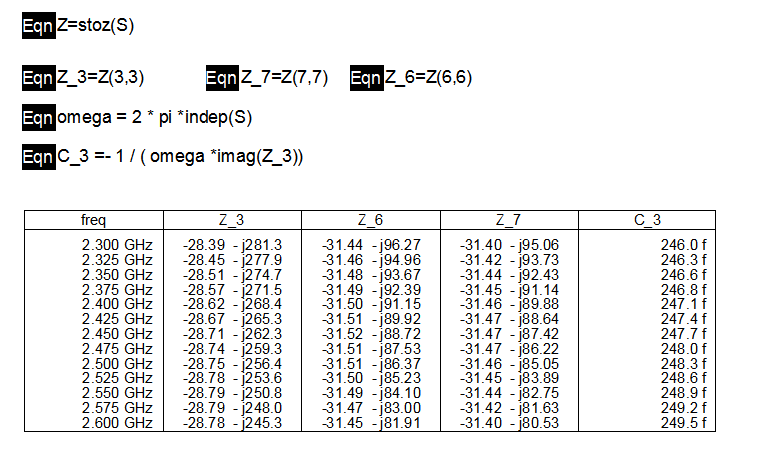
The simulation results are shown in Fig.3.
Please refer to the attachment for the archived workspace files of ADS2016.
To let you help me check the files as conveniently as possible, I also archived the simulated dataset in attachment.
Could you please help me check whether there are some mistakes in my simulation or give me some
explanation why the real part of the impedance of the pad directly connected to the GND plane is so large,
and the imaginary part of the impedance of the pad directly connected to the GND plane is minus?
Thank you very much in advance!
Joshua

Fig.1

Fig.2

Fig.3
I want to use ADS2016 from Keysight to Co-Simulate the PCB layout with RLC.
But for the first step, I found the layout simulation results were not believable.
The real part of the impedance of the pad directly connected to the GND plane seems to be too large,
is about 27.8Ω @f=2.45GHz. And the imaginary part of the impedance of the pad directly connected to the GND plane is minus.
The layout and pins are shown in Fig.1, the pins are automatically added when I converted the PCB file to the ADS files,
and pin type is the none calibration type.
The PCB stack is shown in Fig.2, all PCB material parameters have been set in the simulation file.
The simulation results are shown in Fig.3.
Please refer to the attachment for the archived workspace files of ADS2016.
To let you help me check the files as conveniently as possible, I also archived the simulated dataset in attachment.
Could you please help me check whether there are some mistakes in my simulation or give me some
explanation why the real part of the impedance of the pad directly connected to the GND plane is so large,
and the imaginary part of the impedance of the pad directly connected to the GND plane is minus?
Thank you very much in advance!
Joshua
Fig.1
Fig.2
Fig.3