Continue to Site

Welcome to EDAboard.com

Welcome to our site! EDAboard.com is an international Electronics Discussion Forum focused on EDA software, circuits, schematics, books, theory, papers, asic, pld, 8051, DSP, Network, RF, Analog Design, PCB, Service Manuals... and a whole lot more! To participate you need to register. Registration is free. Click here to register now.

[SOLVED] Whats the purpose of the highlighted cap in this schematic

Status
Not open for further replies.

tajiknomi

Member level 4
Joined
Nov 2, 2015
Messages
79
Helped
0
Reputation
0
Reaction score
0
Trophy points
6
Activity points
754
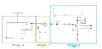
This is overcurrent protection circuit and I have understood its principle but I would like to know why this cap is present at the NPN base? To block AC ? Or it serves some other purpose too ? And what would be the risk involve if this hasn't been present in the first place.

1.png
 

Attachments

  • capture.jpg
    capture.jpg
    33.3 KB · Views: 101

If my academic knowledge is correct its only to block AC.
 

Wrong!

It is there so the bias to the transistor Q1 can't change rapidly. Without it, the latch circuit (Q1,Q2) could trigger on very short pulses from the comparator (stage 2), possibly even during start up when power is first applied.

Brian.
 

It is there so the bias to the transistor Q1 can't change rapidly. Without it, the latch circuit (Q1,Q2) could trigger on very short pulses from the comparator (stage 2), possibly even during start up when power is first applied

Do you means to say that Comparitor will set the output higher for sometime during power up ? Kindly eloborate it a little.
 

The two transistors make a latch circuit. When the base of Q1 rises above Vbe (about 0.6V) it's collector voltage drops and the relay operates. At the same time, Q2 is brought into conduction and provides more base current to Q1 so it stays in 'on' condition. Without the capacitor, the latch would react to any rise in voltage above Vbe and trigger the circuit, even it if was only for a few uS length. What I am saying is the state of the comparator will be indeterminate as the supply voltage rises when the power is turned on and might trigger the latch. The capacitor makes it less responsive so a longer 'high' from the comparator is needed before the latch operates.

What isn't clear from the schematic is what the switch connected to the LED does. If it is a second set of contacts on the relay it stops Q1 and Q2 being a latch and makes them a monostable. When a long enough high comes out of the comparator, the capacitor charges enough to make Q2 conduct, it operates the relay and that disconnects the comparator so no further base current can be provided. There would then be a short delay as the capacitor discharged into Q1 before the relay turned off again. If the comparator output has gone low, it will await a further high before repeating the process, if the comparator output is still high, the circuit will oscillate with the relay turning on and off cyclically.

Brian.
 
Simply see it as a 5 to 10 ms time delay for the overcurrent protection. It disables overcurrent detection for short pulses rather than allowing a higher output. The maximum current for short pulses is only limited by the external circuit and load, which isn't shown in your schematic.
 

What isn't clear from the schematic is what the switch connected to the LED does

The switch shown in the schematic is Normally closed one, as far as i understood it, it is used to reset the latch cycle because once Q1 is activated, it will not deactivate no matter the output from Comparitor is low or high. Pushing the NC switch will drive the base of Q1 low and hence stop the cycle.

- - - Updated - - -

@FVM: My mistake, I should have placed it in the first place.
Capture.PNG
 

I have made that circuit but here is one problem which I am facing right now. I have connected nothing to the Non-inverting pin of the first OP-AMP and whenever i supply the power, it automatically triggers the comparitor and the rest. Does this means that when NON-INVERTING pin is left open, it has higher PD then INVERTING one ?
What should be the best value of resistor so that i can pull down the NON-INVERTING pin in the above case ?
 

Hi,

Does this means that when NON-INVERTING pin is left open, it has higher PD then INVERTING one ?

General rule:
Don't leave any (unused) input floating. This is true for analog circuits as well as for digital circuits.

* The result is not predictable,
* it may cause EMI,
* it may cause increased supply current...

Klaus
 

@KlausST: I have connected 27k resistor to the Non-Inverting pin and it works fine now. But I would be glad to know what value of the resistor should be placed to pull down the pin and what's the general rule for that.
 

Hi,

But I would be glad to know what value of the resistor should be placed to pull down the pin and what's the general rule for that.

Each device has a datasheet. And within this datasheet you find the input specifications.
Maybe for an Opamp.
* input bias current max: 100nA
Now if you want to pull this input to within 10mV(decide your own value) to GND.
Then R = V / I = 10mV / 100nA = 100k
--> use max 100k resistor.

For digital inputs:
If you wan to pull an input to LOW:
* use the datasheet max input leakage current
* use the datasheet max low level input threshold voltage V_IL
--> this gives the max. resistor value you should use

You are free to choose a smaller resistor value.

Klaus
 
But my configuration is like this, input bias current will flow directly to the OpAmp, not through the resistor. Actually, I am using this as a Amplifier.
Capture.PNG

Have I placed the connection to the Non-Inverting pin wrong? I am directly giving the PD at +ve of OpAmp, not via resistor
 
Last edited:

Hi,

But my configuration is like this, input bias current will flow directly to the OpAmp, not through the resistor.
input bias current will always flow directely to the Opamp.

What is this V_CL and resistor circuit?

--> if it is really there, then pin is not floating
--> if it is not there, then bias current is flowing through resistor R

It´s not clear to me what you want to achieve.

Klaus
 

What is this V_CL and resistor circuit?
It´s not clear to me what you want to achieve

Actually, i want to protect another circuit connected in series with the resistor. I am taking the output from a resistor in order to know whether the current exceeds my limit or not. For that, I am using op.amp to amplify this voltage and output the signal to a comparitor which will decide whether to switch ON/OFF the circuit or not [for protection].

Vcl is power source which will drive the circuit which i want to protect.
 

Status
Not open for further replies.

Similar threads

Part and Inventory Search

Welcome to EDABoard.com

Sponsor

Back
Top