Continue to Site

Welcome to EDAboard.com

Welcome to our site! EDAboard.com is an international Electronics Discussion Forum focused on EDA software, circuits, schematics, books, theory, papers, asic, pld, 8051, DSP, Network, RF, Analog Design, PCB, Service Manuals... and a whole lot more! To participate you need to register. Registration is free. Click here to register now.

purpose of diodes in smps

Status
Not open for further replies.

INGLE.SHUBHAM

Member level 1
Joined
Nov 18, 2016
Messages
34
Helped
0
Reputation
0
Reaction score
0
Trophy points
6
Activity points
303
hello every one can anybody tell me what is the purpose of Vr1 and D5 in the circuit and why they are connected in this pattern and how it works in smps design for +12V, 5v with 1A output
and what is the purpose of TNY ic and what is the purpose of optocoupler to trigger the TNY ic
here is the attachment
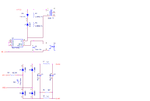


ps.png
 

Hi,

Please read TNY274 datasheet.
There is an "Application" example with full description.
It answers each of your questions - as far as I can see.

If - after reading - there are still some doubts... feel free to ask a detailed question (Question after question, not all at once).

Klaus
 

i understood the purpose of diodes but still getting confused with RF1 and capacitor C3
 

Rf1 is the inrush current limiter.

It adds to the losses, therefore it is only advisable to be employed in low power circuits like this one.

For high power there are other techniques.
 

Rf1 is the inrush current limiter.

It adds to the losses, therefore it is only advisable to be employed in low power circuits like this one.

For high power there are other techniques.

sir can you tell me which are those
 

-NTC thermistors, rated for inrush current duty.
-A time delay relay, which shorts out the inrush limiting resistor.
 

-NTC thermistors, rated for inrush current duty.
-A time delay relay, which shorts out the inrush limiting resistor.

can you please tell me what is the reason of connecting R and c across schottky diode


here is the attachment this is also present in smps circuits.
ps.png

and why they are consider only this values
 

Hi,

The RC across a diode often is used to damp ringing when the diode current becomesclose to zero.
This reduces EMI.

Klaus
 

Hi,

The RC across a diode often is used to damp ringing when the diode current becomesclose to zero.
This reduces EMI.

Klaus

why mosfets are used for high power applications then BJT transistor
 

A bipolar transistor requires some sort of saturation-prevention circuit (i.e. Baker Clamps) to reduce the storage time. That increases static loses, and nevertheless the switching will never be as fast as a Mosfet.
Google or look up Youtube videos on the technique.

BJTs also require to keep a careful eye on SOA.
 
Your top post, you will ahve seen by now, shows diodes needed to prevent fet overvoltage due to leakage inductance discharging into the drain node. Its called a "Primary clamp"
 
can i say that the above power supply is an ASIC design OR no
if NO why?
 

Above power supply is not an ASIC design because power supply is a fly back topology for different application but the IC TNY27 can be call as ASIC design because this IC specifically designed for fly back converter
 

Status
Not open for further replies.

Similar threads

Part and Inventory Search

Welcome to EDABoard.com

Sponsor

Back
Top