Continue to Site

Welcome to EDAboard.com

Welcome to our site! EDAboard.com is an international Electronics Discussion Forum focused on EDA software, circuits, schematics, books, theory, papers, asic, pld, 8051, DSP, Network, RF, Analog Design, PCB, Service Manuals... and a whole lot more! To participate you need to register. Registration is free. Click here to register now.

Inserting clk delay not clk buffer

Status
Not open for further replies.

bit_an

Junior Member level 3
Joined
Mar 11, 2017
Messages
28
Helped
0
Reputation
0
Reaction score
0
Trophy points
1
Activity points
235
Hi,

I have a chain of two flip flops, both triggered by the same clk. I want to configure the clk such that 2nd flip flop gets triggered only in the 2nd positive edge. Any delay is non-synthesizable. How to realize this in rtl design?!

Thanks
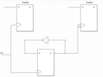
 

Hi,

And what happens on 1st, 3rd, 4th, 5th...pos clock edge?
How to know when to begin with counting? Is there some RST?

A simple sketch could clarify...

Klaus
 

Hi,

The first posedge must trigger ff_1 and 2nd posedge triggers ff_2, next this cycle repeats... I do have a rst in my module.
 

Hi,

The first posedge must trigger ff_1 and 2nd posedge triggers ff_2, next this cycle repeats... I do have a rst in my module.

Clock gating is the easiest way to achieve this. Keep both flops hooked up to the same logical clk signal, but add some counter logic to make sure the second flop has an enable only when the counter has the value you want. The implementation will translate into some ANDed clock logic.
 

A simple sketch could clarify...
Klaus
There is a saying that I've heard, which aptly applies here
...A picture is worth a thousand words...

Hi,
The first posedge must trigger ff_1 and 2nd posedge triggers ff_2, next this cycle repeats... I do have a rst in my module.
Hmm, this is not a picture.

But based on your less than stellar description...Seems like you want this:
Code:
    ___     ___     ___     ___     ___    
___|   |___|   |___|   |___|   |___|   |___
     _______         _______         ______
____/       \_______/       \_______/      
____ _______________ _______________ ______
____x_______________x_______________x______
   ^ <--phase 0--> ^
____________ _______________ ______________
____________x_______________x______________
           ^ <--phase 1--> ^
A toggling clock enable with the first FF enabled on the low phase and the second enabled on the high phase, would seem to fit your description. But the picture is easier to see what is going on.
 

There is a saying that I've heard, which aptly applies here
...A picture is worth a thousand words...


Hmm, this is not a picture.

But based on your less than stellar description...Seems like you want this:
Code:
    ___     ___     ___     ___     ___    
___|   |___|   |___|   |___|   |___|   |___
     _______         _______         ______
____/       \_______/       \_______/      
____ _______________ _______________ ______
____x_______________x_______________x______
   ^ <--phase 0--> ^
____________ _______________ ______________
____________x_______________x______________
           ^ <--phase 1--> ^
A toggling clock enable with the first FF enabled on the low phase and the second enabled on the high phase, would seem to fit your description. But the picture is easier to see what is going on.


RTL code :-

assign DIN = ~QIN;

always @(posedge CLK, RSTB) begin //Intermediate flop
if(RSTB)
QIN <= 1'b0;
else
QIN <= DIN;
end


always @(posedge QIN, RSTB) begin //PHASE 0 flop
if(RSTB)
QP0 <= 1'b0;
else
QP0 <= D0;
end


always @(negedge QIN, RSTB) begin //PHASE 1 flop
if(RSTB)
QP1 <= 1'b0;
else
QP1 <= D1;
end

I assume your RESET is active high and initial state of all flops is 0
 

Attachments

  • eda_ans.PNG
    eda_ans.PNG
    30.3 KB · Views: 89

Status
Not open for further replies.

Part and Inventory Search

Welcome to EDABoard.com

Sponsor

Back
Top