Continue to Site

Welcome to EDAboard.com

Welcome to our site! EDAboard.com is an international Electronics Discussion Forum focused on EDA software, circuits, schematics, books, theory, papers, asic, pld, 8051, DSP, Network, RF, Analog Design, PCB, Service Manuals... and a whole lot more! To participate you need to register. Registration is free. Click here to register now.

[SOLVED] P-FET Power Switch Parallel Diode Question

Status
Not open for further replies.

Batur

Newbie level 4
Joined
Oct 30, 2015
Messages
6
Helped
0
Reputation
0
Reaction score
0
Trophy points
1
Activity points
82
Hi All,

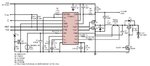
I am trying to design a li-ion charger for a project. I have selected the LTC4008 charger, built and tested the circuit an everything seems fine. However in the reference design found in LTC4008 datasheet there is a schottky diode (D2) connected in parallel to the charge switch as can be seen in the attached picture. I have also tested the circuit without this diode and it still works. It is a fairly large component and I would like to not use it if I can however I can't understand what it does so I would be very gratefull if someone can explain me its purpose.

Best Regards
 

Attachments

  • LTC4008_ref.JPG
    LTC4008_ref.JPG
    94.8 KB · Views: 101

I agree it's strange as it would appear to make the charge switch redundant. It doesn't appear in the application notes that don't have charge switching in them.
I would guess, it is a mistake to show both D2 and Q2, I think they are alternatives but not to be fitted at the same time.

Brian.
 

It's a TVS Diode ( Transient Voltage Suppression ) and it protects the MOS against transient spikes that may possibly occur.
 

Read on page 15 of app note:

The Schottky diode D1, shown in the Typical Application
on the back page, conducts during the dead-time between
the conduction of the two power MOSFETs. This prevents
the body diode of the bottom MOSFET from turning on and
storing charge during the dead-time, which could cost as
much as 1% in efficiency. A 1A Schottky is generally a good
size for 4A regulators due to the relatively small average
current. Larger diodes can result in additional transition
losses due to their larger junction capacitance.
The diode may be omitted if the efficiency loss can be
tolerated.
 

It's a TVS Diode
SBM540 is a 5A schottky diode.

The Schottky diode D1, shown in the Typical Application on the back page, conducts during the dead-time between the conduction of the two power MOSFETs.
The diode in question is D2, not D1.

I don't believe that we'll clarify the question satisfyingly. It looks like that the designer considers the option that the charger is operated for extended time without the series pass transistor activated and didn't want to spend a heat sink for the MOSFET substrate diode operated as rectifier.

Alternative component placement, as suggested would be an explanation, but it should be noted in the schematic.
 
  • Like
Reactions: Batur

    Batur

    Points: 2
    Helpful Answer Positive Rating
Status
Not open for further replies.

Similar threads

Part and Inventory Search

Welcome to EDABoard.com

Sponsor

Back
Top