Toyona Entwined
Newbie level 4
Hi,
So I've taken this fast track Analog course in which we have been assigned a design project. Besides the specs, we were also provided with 2 possible architectures referred from papers, and one of them is a folded cascode.
The problem is we hardly have any idea on how to really approach such design problems because firstly, we are new to analog design and secondly, this is a 1-month course which is usually 4 months. Having slides and such and understanding the smaller parts like the subcircuits isnt helping much because we have hardly gathered any experience/intuition in actually working out similar problems by ourselves.
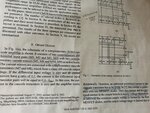
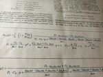
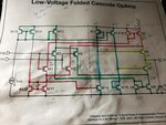
The design consists of complementary diff input pairs (M1, M2 and M3, M4) with complementary current mirrors as active loads. They are in turn connected to a complementary cascode transistors (M7, M8). I have attached pictures of the circuit, specs, and some other related formulas.
I calculated the tail current from Cl and Slew rate (1000uA) but Im not sure as to how I would divide it across the branches. Following the paper I have fixed the ratio of the mirror M10:M9 and M5:M6 to be 1:1.2.
Do I extract the subcircuit components and work them out separately??
I am honestly in a terrible bind here, so IN CASE anyone is willing to help me even further by discussing intensively on how I should analyse the circuit to meet the specs, please feel free to inbox me, I'd be very obliged.
So I've taken this fast track Analog course in which we have been assigned a design project. Besides the specs, we were also provided with 2 possible architectures referred from papers, and one of them is a folded cascode.
The problem is we hardly have any idea on how to really approach such design problems because firstly, we are new to analog design and secondly, this is a 1-month course which is usually 4 months. Having slides and such and understanding the smaller parts like the subcircuits isnt helping much because we have hardly gathered any experience/intuition in actually working out similar problems by ourselves.
The design consists of complementary diff input pairs (M1, M2 and M3, M4) with complementary current mirrors as active loads. They are in turn connected to a complementary cascode transistors (M7, M8). I have attached pictures of the circuit, specs, and some other related formulas.
I calculated the tail current from Cl and Slew rate (1000uA) but Im not sure as to how I would divide it across the branches. Following the paper I have fixed the ratio of the mirror M10:M9 and M5:M6 to be 1:1.2.
Do I extract the subcircuit components and work them out separately??
I am honestly in a terrible bind here, so IN CASE anyone is willing to help me even further by discussing intensively on how I should analyse the circuit to meet the specs, please feel free to inbox me, I'd be very obliged.