Continue to Site

Welcome to EDAboard.com

Welcome to our site! EDAboard.com is an international Electronics Discussion Forum focused on EDA software, circuits, schematics, books, theory, papers, asic, pld, 8051, DSP, Network, RF, Analog Design, PCB, Service Manuals... and a whole lot more! To participate you need to register. Registration is free. Click here to register now.

CMOS two stage amplifier 0.8um technology

Status
Not open for further replies.

thaintrinh

Junior Member level 1
Joined
Apr 8, 2016
Messages
16
Helped
0
Reputation
0
Reaction score
0
Trophy points
1
Activity points
156
Good afternoon.
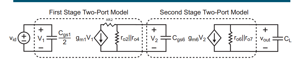
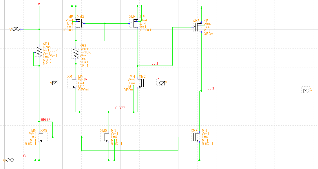
I have been given a circuit like this: note that it has an additional resistor compared to the original one.
1111.PNG
I believe this is a CMOS two stage amplifier in 0.8um technology.
I need to find out the operations, equivalent circuit and Av, Ai, Zin, Zout from this circuit. However, i can do the simulation for this circuit.
None of the documents on the internet seems to help. It would be very helpful if you can help me with this.
Thanks in advance :D
 

I need to find out the operations, equivalent circuit and Av, Ai, Zin, Zout from this circuit. However, i can do the simulation for this circuit.

An equivalent circuit for CMOS two stage amplifiers can be found in every analog circuit design textbook.
If you can simulate the circuit, you should be able to find the parameters. So what's your problem?
 

It's a "strange" Differential Pair with an Output Stage amplifier.
PMOS and NMOS device cannot have a same dimension for a proper operation.Here, every MOS has 4um/4um..Weird..
 

An equivalent circuit for CMOS two stage amplifiers can be found in every analog circuit design textbook.
If you can simulate the circuit, you should be able to find the parameters. So what's your problem?

I just don't know where to put that additional resistor in this equivalent circuit to compute all that parameters.
equivalent circuit.PNG
And I have to make comparison between my calculation and simulation.
 

I just don't know where to put that additional resistor in this equivalent circuit to compute all that parameters.
Between the current source gm1V1 and the output resistance ro2||ro4. But at a branch current of about 2µA this XR2 10kΩ resistor is negligible, I'd say; it is dispensable, anyway.
 
Between the current source gm1V1 and the output resistance ro2||ro4. But at a branch current of about 2µA this XR2 10kΩ resistor is negligible, I'd say; it is dispensable, anyway.

Thanks a lot :D I am not really good with these kind of circuits and stuff :(.
So, the XR2 will stay in parallel with the current source and the output resistance ro2||ro4 ?
The value of that resistor is not really important since I'm trying to compute everything "in theory" :D.
Thank you for answering these stupid questions of mine.
 

One more small question here,
If i put the resistor in this position
case 2.PNG
I'm trying to determine Rout1 using the impact of the current mirror feedback,
So, is it gonna be: Rout1 = (ro2 + XR2) || ro4 ?
and if the position of XR2 is in the upper position, Rout1 = ro2 || (ro4 + XR2) ?
Thanks a million
 

View attachment 139345 So, is it gonna be: Rout1 = (ro2 + XR2) || ro4 ?
Yes, I think so.

... and if the position of XR2 is in the upper position, Rout1 = ro2 || (ro4 + XR2) ?
No, I don't think so: XR2 in this previous position has nothing to do with the (ro2 || ro4) output impedance of the 1st stage. It just diminishes the current of the XM1-XM3 stage (a very little bit: in the order of XR2/(1/gm1)≈XR2/ro1 ). So you could replace the current source (gm1V1) by (V3/((1/gm1)+XR2)) and remove again the XR2 symbol in the equivalent circuit schematic.
 
Hence, for the first position, I just replace (ro2 || ro4) with (ro2 + XR2) || ro4 in this equivalent circuitView attachment 139318
This is the second position that i was talking about in my previous reply
upper right branch.PNG
v3 you mentioned is vg3 = (gm1 / gm3 ) * (Vid/2)
I thought XR2 has nothing to do with this vg3 ?
Thank you for your patience :D
 

Hence, for the first position, I just replace (ro2 || ro4) with (ro2 + XR2) || ro4 in this equivalent circuit
NO: if this is your first position:
... didn't you read my above explanation (properly)?

replace the current source (gm1V1) by (V3/((1/gm1)+XR2)) and remove again the XR2 symbol in the equivalent circuit schematic.
v3 you mentioned is vg3 = (gm1 / gm3 ) * (Vid/2)
What is (Vid/2) ?

I thought XR2 has nothing to do with this vg3 ?
I think you've mixed that up:
XR2 in this previous position has nothing to do with the (ro2 || ro4) output impedance of the 1st stage.
Read more thoroughly, please!

This is the second position that i was talking about in my previous reply
View attachment 139364
... I just replace (ro2 || ro4) with (ro2 + XR2) || ro4 in this equivalent circuit
No, again: you should replace (ro2 || ro4) by (ro2 || (ro4 + XR3))
You changed the out1 connection point!
 

God, i think i just messed everything up.
Thank you for your explanation.
I will run the analysis again thoroughly, can you judge it for me pls?
Thanks a million :(
 

Sorry, I'm quite hopeless now :bang:
This is my circuit, can you derive the equation for Av, Vo1 and Zout1 for me pls,
Thanks a million times case 1.jpg
 

Thank you again for your patience.
I've read all those textbooks.
For all the cases i'm going to consider, I have a differential voltage +Vid/2 applied to XM1 (Gate) and -Vid/2 to XM2 (Gate).
And I this case to consider: the additional resistor is put between XM3 and XM1 like this 7352457800_1497363496.png
Why in this case, as you said, replace (gm1V1) by (V3/((1/gm1)+XR2))?
Correct me if i'm wrong, here's my analysis:
+ The current source that represents XM1 is calculated as gm1*Vgs1 = gm1*Vid/2.
+ Hence, Vg3 = -gm1*((ro1 + XR2) || ro3 || (1/gm3))*Vid/2, since ro1, ro3 >> 1/gm3 => Vg3 = -gm1/gm3 * Vid/2 => XR2 has nothing to do with the voltage gain (Av) of this opamp circuit. I assume that V3 you wrote is Vg3 ?
+ In my equivalent circuit, V1 is Vid through a input impedance Zin (which is infinite) => V1 = Vid ?
+ In my simulation, as XR2 increases, Av increases as well ?
Can you explain for me pls, thank you very much.
 
Last edited:

For all the cases i'm going to consider, I have a differential voltage +Vid/2 applied to XM1 (Gate) and -Vid/2 to XM2 (Gate).
And I this case to consider: the additional resistor is put between XM3 and XM1 like this View attachment 139524
Why in this case, as you said, replace (gm1V1) by (V3/((1/gm1)+XR2))?
I just replaced your current source by a current source which included XR2 .


I assume that V3 you wrote is Vg3 ?
Right.


Correct me if i'm wrong, here's my analysis:
+ The current source that represents XM1 is calculated as gm1*Vgs1 = gm1*Vid/2.
+ Hence, Vg3 = -gm1*((ro1 + XR2) || ro3 || (1/gm3))*Vid/2, since ro1, ro3 >> 1/gm3 => Vg3 = -gm1/gm3 * Vid/2 => XR2 has nothing to do with the voltage gain (Av) of this opamp circuit.
+ In my equivalent circuit, V1 is Vid through a input impedance Zin (which is infinite) => V1 = Vid ?
You didn't yet explain neither V1 nor Vid.
And I must admit I don't feel quite fit with those equivalent circuits.

+ In my simulation, as XR2 increases, Av increases as well ?
Yes, about the same as the left branch current decreases:
a very little bit: in the order of XR2/(1/gm1)≈XR2/ro1
... as I indicated above.
 
Status
Not open for further replies.

Part and Inventory Search

Welcome to EDABoard.com

Sponsor

Back
Top