Continue to Site

Welcome to EDAboard.com

Welcome to our site! EDAboard.com is an international Electronics Discussion Forum focused on EDA software, circuits, schematics, books, theory, papers, asic, pld, 8051, DSP, Network, RF, Analog Design, PCB, Service Manuals... and a whole lot more! To participate you need to register. Registration is free. Click here to register now.

PCB Assemblers must be requested to test PCBs that they assemble?

Status
Not open for further replies.
T

treez

Guest
Hello,
We have had 1000 offline, DALI dimmable LED driver PCBs made up. We did not request for the PCB assembler to do any testing whatsoever of the finished PCBs.
We are finding that some of the PCBs work and dim according to the commands but some don’t. Some Dim according to the commands on the first power up, but then don’t on the second power up and not thereafter either.
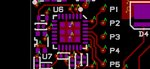
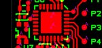
We cannot actually check the DALI signal is actually getting to the microcontroller pin because the PIC18F26K20 pins are too small and hidden to get to the pin (28 QFN package)….so we have to go on the nearest 0402 resistor etc.
I am wondering if the PCBs have been badly assembled? Maybe they did not use the correct amount of paste on each of the circuit pads, and maybe the reflow baths weren’t hot enough? Maybe we have dry, intermittent joints all over the PCBs? –The fact that we didn’t ask the PCB assemblers to do any PCB testing for us meant that they had no way of knowing if they had set the reflow temperature correctly, no way of knowing if they had used the correct amount of paste for each pad etc.
Do you believe it is always essential to request that the PCB assemblers do PCB tests, if for no other reason than it shows them if their assembly process is good or not? After all, if they can’t test the PCBs , then how would they know that they are assembling them wrong.

Do you agree that PCB assembly is not an exact science, and that the Assemblers needs tests on the PCBs to tell them if their assembly process is right or wrong?
Not requesting the PCB assembler to do tests on finished PCBs is surely bad practice?
 

PCB assembly -should- be an exact science but may take
science (experimentation, analysis, feedback, repeat) to
get there. A blind stab is not science. Now comes the fun
of collecting all of the failure signatures and rooting out
their causes. Your conjectural questions are asking for
failure analysis based answers, board by board, followed
by some analysis looking for common cause(s).

If you request testing you must be prepared to pay the
test development and test process costs. This is going
to hurt. But it is also the only real way to cause vendor
learning - make them ship tested-good parts and feel
pain until they do. And make them responsible for the
BOM parts procurement as well, no paying for stuff they
break while floundering.

But you'll get a NRE bill months before you see any
product. And you will probably have to chip in some
expert engineer time from the product development
group to help the test engineer develop the test
solution, another cost element.

Seems like someone did not think ahead to debug phase
and this might also affect test costs - lack of access
leads to extra complicated programs and poor test
coverage (not to mention bench test headaches as you
relate).
 
  • Like
Reactions: treez

    T

    Points: 2
    Helpful Answer Positive Rating
Thanks, to make matters worse, when you are probing the board so as to investigate its faults, the 0402's are too small for free scope probing, and you have to solder flying wires to the board so you can probe it....these flying wires very often couple so much noise into the board that it stops working. (by 'working' i mean lighting the leds........most boards dont light the leds to the correct dimming level, so they are not really 'working', just 'working' in kind)

The other day i was powering the PCB off the mains isolation transformer, and i soldered flying wires in so that i could view the DALI signal that enters the micro.........the flying wires literally stopped the board from working (ie turned the leds off)....then i found i could start the board working again (ie turn the leds back on) by literally clipping the scope earth lead to the circuit ground connected flying wire. (The ‘circuit ground’ is actually the negative output of the mains bridge rectifier. The PCB sits on an earthed heatsink, and has an insulation pad between PCB and heatsink).
It was weird being able to smartly turn the LEDs on and off by clipping/unclipping the scope earth lead clip to the “circuit ground”.

The PCB has no mains isolation on it (no SMPS transformer, etc)

- - - Updated - - -

But you'll get a NRE bill months before you see any
product.
Thanks, though i mean just a very simple test like
1.."load test code into micro"
2..Apply mains to connector A
3..Check if LEDs come on and dim up and down

- - - Updated - - -

Strangely we have one board, which works perfectly every time we power it up. It always correctly responds to the DALI dimming signals.
I am wondering if this board is the one that has all the pads of its microconctoller correctly soldered (no dry joints). It strikes me that if on the other boards the micro pads that are inputs are dry joint, then that input will be picking up noise and probably resulting in bad behaviour….probably triggering interrupts and all sorts.
Do you think dry joints of the micro pads is a likely cause of our problems?

- - - Updated - - -

I wrote test code for the board so I could see if the pin that gets used for DALI signal input actually works. My test code literally just receives an input into the pin, then outputs the same high or low signal on another pin which I made an output. (the output pin is the pin that normally gives out the PWM dimming signal in accordance with the received DALI dimming signal).

However, my test code doesn’t work, and I don’t know if its not working because the micro is broke/dry joint, or my code is bad.
I am sure my test code is logically correct, but maybe I have some syntax error somewhere? There doesn’t seem to be a manual for PIC18F26K20 which tells you what the syntax needs to be for all the “set-up” code that you have to write.
This thread concerns my test code...
https://www.edaboard.com/showthread.php?t=368575
 

Without design for testability, there is little sense in arbitrary tests performed by the assembly house.

Although it's possible to mess up even a little PCB by incorrect processing, e.g. wrong reflow profile, inappropriate solder mask parameters, it's very unlikely to get such a low production yield. Considering your previous threads about the same product, it looks more like some fundamental design fault.

Solder joint quality can be perfectly assessed by optical inspection or X-ray. In case of doubt make a microsection of a failed board. Intermittent failure can be a problem, but if a small board refuses correct operation permanently, it's usually possible to trace the primary fault down to component and pin level.
 
  • Like
Reactions: treez

    T

    Points: 2
    Helpful Answer Positive Rating
it looks more like some fundamental design fault.
But the boards and software are all the "same", and one of them works perfectly...so its surely unlikely to be a design fault?
The LED drivers are simple linear regulator type, so its not a complex design.
Solder joint quality can be perfectly assessed by optical inspection or X-ray. In case of doubt make a microsection of a failed board.
Thanks, as you know, optical inspection is off the menu for us because its a 28QFN package...the pads are under the component body.
 
Last edited by a moderator:

Without knowing the physical size and layout of your product it is difficult to advise but it sounds like your PCB designer didn't build "testability" into the layout. Normal practice is to leave small test pads at critical places on the board. These need only be 1mm to 2mm diameter, just big enough to hit with a pointed probe. For 1K runs they can be hand probed but for more than that I would consider some automated testing, possibly a bed-of-nails to make connections and either external control signals or an internal self-test to demonstrate it works properly. A well designed self-test would enable you to isolate the functionality of different circuit sections so you can make a better and quicker diagnosis of failures.

Stressing that I have no idea what your product looks like or it's circuitry, this is what I would look towards making:

1. a test rig with tooling pins to fit mounting holes. This is to accurately locate the PCB on the rig.
2. spring probes at positions to match the inputs, outputs and test pads.
3. a suitably protected power source and load to apply to the board.
4. either some self-test trigger which can demonstrate all the functions are working or externally applied stimulus that runs it through all its functions.

Compared to the cost of returns/repairs and bad reputation it is a good investment. I've done this on products ranging from power tool speed controllers and mobile phones up to PC motherboards, ~10 probes up to more than 1,000. If you can, get the PCB manufacturer to make a drilled blank board, one with all the holes but no copper at all, when glued to a thicker backing it makes a cheap but accurate template for mounting test probes.

Brian.
 

optical inspection is off the menu for us because its a 28QFN package...the pads are under the component body.

Just wrong. Did you ever look closely on an assembled QFN part?

Any industry standard QFN footprint has the pads protruding the case shape by some amount, e.g. huge 0.35 mm in the Microchip suggested footprint. The pins are also extending on the package lateral surface with 0.2 mm height, you can e.g. perform an electrical continuity test of the solder joint, also re-solder it if necessary.
 

Thanks , our 28QFN is on pages 433,434 of the PIC18F26K20 datasheet
**broken link removed**
….from what I can see, the pad “should” protrude 0.2mm out from the package outline. On our board, I don’t remember seeing any such copper protrusion…I am now wondering if the layout guy has made the pads too small and we are sitting them on top of solder resist.
 

Judging by your other posts, my guess is that you left PGM pin RB5 floating (or connected to circuit in a way that it can go high) and LVP turned on.

That might well cause some boards to work, others to not work, and others to be intermittent.

Pure guess work though, as I have not seen your schematic.
 

If the footprint isn't following industry standard suggestions, I wonder what can be else wrong with the layout?

You can clarify by inspecting the gerber files. Regarding Microchip datasheet, I calculate 6.7 mm outer footprint width (C2=5.7 mm center line distance + Y1=1.00 mm pad length). QFN package is 6 x 6 mm. Gives 0.35 mm protrusion on each side.

- - - Updated - - -

That's how an assembled QFN should look like

QFN32.jpg

By working of the protruding pads and lateral pin metal, a solder meniscus is formed at each pin. The good joint quality is obvious at first sight.
 

Thankyou very much, i dont remember ours being anything like as good as what you kindly show.
In fact i remember having to solder a kynar wire to one of the pins directly, it took me about an hour to do, and i dont rememeber seeing any protruding pad bits, i certainly dont recall seeing a pad solder-meniscus going up the pad metal on the side of the IC....i just remember a bare pad extending up the side of the IC with no solder on it at all....definetely no meniscus of solder. i will now check the gerbers.

- - - Updated - - -

The footprints of Topelec, TopPaste and TopResist of our PIC18F26K20 is as attached.
The footprint edge to edge of copper is 6.6mm, so this is close enough to the recommended footprint of 6.7mm to be OK.
What is concerning is that the recommended “gap” between the centre gnd pad and the pins is just 0.225mm…..i am wondering if our PCB assemblers have slightly misplaced the chips, and the pin pads are very slightly impinging on the centre copper pad.

- - - Updated - - -

The also attached image showing the top paste layer and topelec layer together shows that there are two 0.4mm vias in the centre pad of the PIC18F26K20 microcontroller (marked ‘A’).
I believe that these can drag the IC off centre when it is reflow soldered. Do you agree?
If our PIC18F26K20 gets dragged off centre then its pin pads will short to the centre ground pad. Do you agree?
Also, I don’t see how they can get a solder resist mask “bridge” in the gap between the centre pad and the pin pads….the gap is just 0.225mm.

- - - Updated - - -

Also, the gap between the solder mask openings of adjacent pins is just 0.1mm wide....i simply cannot believe that it is possible to spray a "sliver" of solder resist into such a tiny gap?
The gap between the mask of the pins and the centre pad is just 0.22mm...and again i simply dont believe it is possible to spray solder resist into such a tiny gap without getting it over the edge of the mask openings?
 

Attachments

  • PIC18F26K20 _topelec.jpg
    PIC18F26K20 _topelec.jpg
    64.8 KB · Views: 84
  • PIC18F26K20 _Toppaste.jpg
    PIC18F26K20 _Toppaste.jpg
    34.7 KB · Views: 86
  • PIC18F26K20 _topResist.jpg
    PIC18F26K20 _topResist.jpg
    67.4 KB · Views: 81
  • Vias in PIC18F26K20 centre pad_.jpg
    Vias in PIC18F26K20 centre pad_.jpg
    134.7 KB · Views: 80

Pin 16 worries me.
Why isn't it connected to the middle ground area. It looks like the two VSS pins are not linked together unless it is through a loop of tracks somewhere off the image.

As predicted, there is no pull-down on PGM, pull-up on VPP or static protection on the other pins.

Brian.
 

Pin 16 worries me.
Why isn't it connected to the middle ground area. It looks like the two VSS pins are not linked together unless it is through a loop of tracks somewhere off the image.
Thanks yes, it is indeed through a loop of tracks that come back to the vias in the centre gnd pad....i am not sure why they didnt just link it from 16 to centre pad though.

- - - Updated - - -

As predicted, there is no pull-down on PGM,
Thanks, the PGM issue we sorted out now, but still have the problems...we have defined it LVP OFF and have the pin declared as output....btu we still have the malfunction issue.

- - - Updated - - -

(no) pull-up on VPP
Thansk, yes , we do the 4k7 pullup on vpp as a wired in external modification...as well as the 10n cap top ground from Vpp pin.

- - - Updated - - -

static protection on the other pins
Thanks, do you mean that there's no series resistors into the micro pins?
 

There are many types of design error which can manifest
as intermittent or probabilistic failures. Floating pins are
a prime example, state determined by leakage and/or
non-determinstic charging. That one piece works, does
not prove the robustness of the design or its workmanship.
Only that there is a chance of not-failing.

Since you're on about solder joints, you should go inspect
some at high magnification relative to the picture shown,
for qualities. You can find references to solder joint
inspection criteria which would point you to likely "recipe"
causes, if you find non-perfect ones. Likewise inspection
should show you whether your lands are properly oversized
and whether the component is being placed correctly.

But seems like several basic hookup issues have already
been called out. These should be run down before you
go and blame the manufacturer else you'll look like a
kook and put them on defensive permanently rather
than for proper cause.

Simple test or full bed of nails test, you are going to be
charged by anyone running a rational business. How
much, may depend on level of effort but effort -will-
be paid one way or the other (NRE, per unit, or likely
both).

What you are asking for here, is basically a freebie FMEA
and failure analysis. I might recommend that you do this
more formally within your own shop. Assign a competent
but as-yet-uninvolved engineer to attack the design looking
for issues such as these ones raised, but thoroughly (you
can't expect thoroughness nor access to details from this
pool of enthusiasts) but you can task someone to be the
"red team" and see how many ways they can find to break
your design. From this you gain both fixes, and learning at
the institutional (design team, product line, best practices)
level.

Your career as a designer depends more on how you respond
to failure, than how many immediate successes. Everybody's
a star until they aren't anymore. Start planning your comeback
unless you want to spend the rest of your life doing late night
infomercials.
 
Last edited:

Hello, as you c an see in the attached JPEG, “Via too close to pad”, there is a 0.4mm drill via next to pin 10 of the 28 pin microcontroller. This is surely way too close? (the centre of the via is 0.5mm away from the edge of the pad of pin10.
Can this result in the microcontroller getting pulled off the centre of its footprint during the reflow process?

- - - Updated - - -

Also, in the attached screen shot from the PCB ("Vias too close to SOT23-5 opamp pads"), we have 0.4mm drill vias whose centre is just 0.5mm away from the edge of the pads of a SOT23-5 opamp. Do you believe that this is too close and that solder can be wicked away from the joint and result in dry joints?
 

Attachments

  • Via too close to pad.jpg
    Via too close to pad.jpg
    103.7 KB · Views: 76
  • Vias too close to SOT23-5  opamp pads.JPEG
    Vias too close to SOT23-5 opamp pads.JPEG
    66.9 KB · Views: 114

It isn't ideally placed but the opposite of what you suggest is more likely to happen. When all the solder is liquid, it's cohesive attraction tends to drift the IC to the center of the pads, essentially it becomes 'self centering'.

That VSS loop is bad news though, good design would make VSS impedances as small as possible, in this case linking to the middle ground area as with pin 5. It isn't a resistance issue, it's that the clock and maybe other signals can become noisy with unpredictable consequences.

I fully agree with Dick's analysis of the design strategy, you really should scrutinize all designs for electrical and layout problems before taking to manufacturing stage. At very least, make a few prototypes by hand, it's slow work but nowhere near as time consuming or costly as having 1,000 dud boards on your hands.

Brian.
 

It don't understand the worries about "via too close to pad". According to gerber data, there's no solder mask opening for this vias. So unless the gerber data have been edited during PCB production, there's no chance to drain solder here. Via in exposed pad is a permanent discussion point in design rule checks. I tend to allow small open vias (0.3 mm or below), in some cases they must be tented, e.g. any PCB with double side SMD placement.

Analyzing the actual circuit faults answers empirically if the PCB design has problems.
 

Status
Not open for further replies.

Part and Inventory Search

Welcome to EDABoard.com

Sponsor

Back
Top