Continue to Site

Welcome to EDAboard.com

Welcome to our site! EDAboard.com is an international Electronics Discussion Forum focused on EDA software, circuits, schematics, books, theory, papers, asic, pld, 8051, DSP, Network, RF, Analog Design, PCB, Service Manuals... and a whole lot more! To participate you need to register. Registration is free. Click here to register now.

Very simple XC8 C code for PIC18F26K20 doesnt work

Status
Not open for further replies.
T

treez

Guest
Hello,
The following XC8 C code for PIC18F26K20 Builds successfully but doesn’t work. Please help make it work?
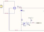
All it is supposed to do is output on RC2 what it reads as an input on RB0. (they are both Digital I/O ports)
I cannot see why it wont work.
The following is the crux of the entire code………..

while(1) {
if (PORTBbits.RB0 == 0) {PORTCbits.RC2 = 0;}
__delay_ms(1);
if (PORTBbits.RB0 == 1) {PORTCbits.RC2 = 1;}
__delay_ms(1);
}
…..surely there is nothing wrong with this?
Here is the complete code listing……

Code:
/*
 * File:   main.c
 */

//This file is very simple code.
//It simply puts out on RC2 what it reads on RB0. (HIGH or LOW)
/*
  Generated Main Source File
  File Name:
    main.c

  Description:
 *     Generation Information :
        Device            :  PIC18F26K20
    The generated drivers are tested against the following:
        Compiler          :  XC8 v1.38
        MPLAB             :  MPLAB X IDE v3.61
 */


#include <xc.h>
#include <stdint.h>
#include <stdlib.h>

#define _XTAL_FREQ  16000000

// CONFIG1H
#pragma config FOSC = INTIO67   // Oscillator Selection bits (Internal oscillator block, port function on RA6 and RA7)
#pragma config FCMEN = OFF      // Fail-Safe Clock Monitor Enable bit (Fail-Safe Clock Monitor disabled)
#pragma config IESO = OFF       // Internal/External Oscillator Switchover bit (Oscillator Switchover mode disabled)

// CONFIG2L
#pragma config PWRT = OFF       // Power-up Timer Enable bit (PWRT disabled)
#pragma config BOREN = OFF      // Brown-out Reset Enable bits (Brown-out Reset disabled in hardware and software)
#pragma config BORV = 18        // Brown Out Reset Voltage bits (VBOR set to 1.8 V nominal)

// CONFIG2H
#pragma config WDTEN = OFF      // Watchdog Timer Enable bit (WDT is controlled by SWDTEN bit of the WDTCON register)
#pragma config WDTPS = 32768    // Watchdog Timer Postscale Select bits (1:32768)

// CONFIG3H
#pragma config CCP2MX = PORTC   // CCP2 MUX bit (CCP2 input/output is multiplexed with RC1)
#pragma config PBADEN = OFF     // PORTB A/D Enable bit (PORTB<4:0> pins are configured as digital I/O on Reset)
#pragma config LPT1OSC = OFF    // Low-Power Timer1 Oscillator Enable bit (Timer1 configured for higher power operation)
#pragma config HFOFST = OFF     // HFINTOSC Fast Start-up (The system clock is held off until the HFINTOSC is stable.)
#pragma config MCLRE = ON       // MCLR Pin Enable bit (MCLR pin enabled; RE3 input pin disabled)

// CONFIG4L
#pragma config STVREN = OFF     // Stack Full/Underflow Reset Enable bit (Stack full/underflow will not cause Reset)
#pragma config LVP = ON         // Single-Supply ICSP Enable bit (Single-Supply ICSP enabled)
#pragma config XINST = OFF      // Extended Instruction Set Enable bit (Instruction set extension and Indexed Addressing mode disabled (Legacy mode))

// CONFIG5L
#pragma config CP0 = OFF        // Code Protection Block 0 (Block 0 (000800-003FFFh) not code-protected)
#pragma config CP1 = OFF        // Code Protection Block 1 (Block 1 (004000-007FFFh) not code-protected)
#pragma config CP2 = OFF        // Code Protection Block 2 (Block 2 (008000-00BFFFh) not code-protected)
#pragma config CP3 = OFF        // Code Protection Block 3 (Block 3 (00C000-00FFFFh) not code-protected)

// CONFIG5H
#pragma config CPB = OFF        // Boot Block Code Protection bit (Boot block (000000-0007FFh) not code-protected)
#pragma config CPD = OFF        // Data EEPROM Code Protection bit (Data EEPROM not code-protected)

// CONFIG6L
#pragma config WRT0 = OFF       // Write Protection Block 0 (Block 0 (000800-003FFFh) not write-protected)
#pragma config WRT1 = OFF       // Write Protection Block 1 (Block 1 (004000-007FFFh) not write-protected)
#pragma config WRT2 = OFF       // Write Protection Block 2 (Block 2 (008000-00BFFFh) not write-protected)
#pragma config WRT3 = OFF       // Write Protection Block 3 (Block 3 (00C000h-00FFFFh) not write-protected)

// CONFIG6H
#pragma config WRTC = OFF       // Configuration Register Write Protection bit (Configuration registers (300000-3000FFh) not write-protected)
#pragma config WRTB = OFF       // Boot Block Write Protection bit (Boot Block (000000-0007FFh) not write-protected)
#pragma config WRTD = OFF       // Data EEPROM Write Protection bit (Data EEPROM not write-protected)

// CONFIG7L
#pragma config EBTR0 = OFF      // Table Read Protection Block 0 (Block 0 (000800-003FFFh) not protected from table reads executed in other blocks)
#pragma config EBTR1 = OFF      // Table Read Protection Block 1 (Block 1 (004000-007FFFh) not protected from table reads executed in other blocks)
#pragma config EBTR2 = OFF      // Table Read Protection Block 2 (Block 2 (008000-00BFFFh) not protected from table reads executed in other blocks)
#pragma config EBTR3 = OFF      // Table Read Protection Block 3 (Block 3 (00C000-00FFFFh) not protected from table reads executed in other blocks)

// CONFIG7H
#pragma config EBTRB = OFF      // Boot Block Table Read Protection bit (Boot Block (000000-0007FFh) not protected from table reads executed in other blocks)

    
void main(void)
{
    
    OSCCON = 0x72;          // 16MHz
    OSCTUNE = 0x00;
    
    //Set up Special Function  Registers
    ANSEL = 0x00;   //Enable all input buffers (not using analog functions)
    ANSELH = 0x00;  //Enable all input buffers (not using analog functions)
    
    ADCON0 = 0x00;   //ADC disabled
    
    CM2CON0 = 0x00; //Comparator 2 disabled
    CM1CON0 = 0x00;  //Comparator 1 disabled
    
    CCP2CON = 0x00;  //Disable PWM and capture compare modules.
    
    CVRCON = 0x00;  //Disable internal voltage reference (of comparator))
    
    TRISA = 0b00000110;     //AJM checked
    TRISB = 0b00001111;      //AJM checked       //RB0 is input.
    TRISC = 0b00000000;     //AJM checked.      //RC2 = Output.
   
    INTCON = 0x00;  //Disable all interrupts
    INTCON2 = 0x80; //Disable PORTB pullups
 
    SLRCON = 0x00;     //All PORTB outputs slow at standard rate.
   
    PORTCbits.RC2 = 0;      //LEDs OFF
    
    while(1) {
    if (PORTBbits.RB0 == 0) {PORTCbits.RC2 = 0;}
    __delay_ms(1);
    if (PORTBbits.RB0 == 1) {PORTCbits.RC2 = 1;}
    __delay_ms(1);
    }

    return;
}
 

hello

use of LAT instead of PORT for 18F ...
increase Delay if you want to see the effect
check once if RC2 bit change .. it means programme is running


Code:
LATCbits.RC2=0;
__delay_ms(1000);
LATCbits.RC2=1;
__delay_ms(1000);
LATCbits.RC2=0;

while(1) {
    if (PORTBbits.RB0 == 0) {LATCbits.RC2 = 0;}
    __delay_ms(1000);
    if (PORTBbits.RB0 == 1) {LATCbits.RC2 = 1;}
    __delay_ms(1000);
 
Last edited:

It wont allow LAT to be used.....mplab gives error
I am using also pic18f26k20 and xc8 compier and LAT is working just fine. Below you can see a part of the code.


Code:
#define LAMP_EN_PIN         LATAbits.LATA7
#define LAMP_EN_PIN_TRIS    TRISAbits.TRISA7

LATA = 0;
LATB = 0;
LATC = 0;
LAMP_EN_PIN_TRIS = 0;
LAMP_EN_PIN = 1;
 

Thanks, here is the latest code, though it still doesnt work.
The code is so simple and obviously logically correct....theres either a syntax error, or the setup hasnt been done properly, or the micro is dead, surely?
Do you see any mistakes?
All this test code does is read an input on one pin, and put out the same state on a different pin....

Do you know what is the guidelines for setting the CONFIG bit LVP?

We do ICSP and power the PIC from the Pickit3 during programming....in operation the micro has a 2V5 supply.

Code:
/*
 * File:   main.c
 */

//This file is very simple code.
//All it does is mimick the input on pin 18 (RB0) and put it out on pin 10 (RC2))
/*
  Generated Main Source File
  File Name:
    main.c

  Description:
 *     Generation Information :
        Device            :  PIC18F26K20
    The generated drivers are tested against the following:
        Compiler          :  XC8 v1.38
        MPLAB             :  MPLAB X IDE v3.61
 */


#include <xc.h>
#include <stdint.h>
#include <stdlib.h>

#define _XTAL_FREQ  16000000

// CONFIG1H
#pragma config FOSC = INTIO67   // Oscillator Selection bits (Internal oscillator block, port function on RA6 and RA7)
#pragma config FCMEN = OFF      // Fail-Safe Clock Monitor Enable bit (Fail-Safe Clock Monitor disabled)
#pragma config IESO = OFF       // Internal/External Oscillator Switchover bit (Oscillator Switchover mode disabled)

// CONFIG2L
#pragma config PWRT = OFF       // Power-up Timer Enable bit (PWRT disabled)
#pragma config BOREN = OFF      // Brown-out Reset Enable bits (Brown-out Reset disabled in hardware and software)
#pragma config BORV = 18        // Brown Out Reset Voltage bits (VBOR set to 1.8 V nominal)

// CONFIG2H
#pragma config WDTEN = OFF      // Watchdog Timer Enable bit (WDT is controlled by SWDTEN bit of the WDTCON register)
#pragma config WDTPS = 32768    // Watchdog Timer Postscale Select bits (1:32768)

// CONFIG3H
#pragma config CCP2MX = PORTC   // CCP2 MUX bit (CCP2 input/output is multiplexed with RC1)
#pragma config PBADEN = OFF     // PORTB A/D Enable bit (PORTB<4:0> pins are configured as digital I/O on Reset)
#pragma config LPT1OSC = OFF    // Low-Power Timer1 Oscillator Enable bit (Timer1 configured for higher power operation)
#pragma config HFOFST = OFF     // HFINTOSC Fast Start-up (The system clock is held off until the HFINTOSC is stable.)
#pragma config MCLRE = ON       // MCLR Pin Enable bit (MCLR pin enabled; RE3 input pin disabled)

// CONFIG4L
#pragma config STVREN = OFF     // Stack Full/Underflow Reset Enable bit (Stack full/underflow will not cause Reset)
#pragma config LVP = ON         // Single-Supply ICSP Enable bit (Single-Supply ICSP enabled)
#pragma config XINST = OFF      // Extended Instruction Set Enable bit (Instruction set extension and Indexed Addressing mode disabled (Legacy mode))

// CONFIG5L
#pragma config CP0 = OFF        // Code Protection Block 0 (Block 0 (000800-003FFFh) not code-protected)
#pragma config CP1 = OFF        // Code Protection Block 1 (Block 1 (004000-007FFFh) not code-protected)
#pragma config CP2 = OFF        // Code Protection Block 2 (Block 2 (008000-00BFFFh) not code-protected)
#pragma config CP3 = OFF        // Code Protection Block 3 (Block 3 (00C000-00FFFFh) not code-protected)

// CONFIG5H
#pragma config CPB = OFF        // Boot Block Code Protection bit (Boot block (000000-0007FFh) not code-protected)
#pragma config CPD = OFF        // Data EEPROM Code Protection bit (Data EEPROM not code-protected)

// CONFIG6L
#pragma config WRT0 = OFF       // Write Protection Block 0 (Block 0 (000800-003FFFh) not write-protected)
#pragma config WRT1 = OFF       // Write Protection Block 1 (Block 1 (004000-007FFFh) not write-protected)
#pragma config WRT2 = OFF       // Write Protection Block 2 (Block 2 (008000-00BFFFh) not write-protected)
#pragma config WRT3 = OFF       // Write Protection Block 3 (Block 3 (00C000h-00FFFFh) not write-protected)

// CONFIG6H
#pragma config WRTC = OFF       // Configuration Register Write Protection bit (Configuration registers (300000-3000FFh) not write-protected)
#pragma config WRTB = OFF       // Boot Block Write Protection bit (Boot Block (000000-0007FFh) not write-protected)
#pragma config WRTD = OFF       // Data EEPROM Write Protection bit (Data EEPROM not write-protected)

// CONFIG7L
#pragma config EBTR0 = OFF      // Table Read Protection Block 0 (Block 0 (000800-003FFFh) not protected from table reads executed in other blocks)
#pragma config EBTR1 = OFF      // Table Read Protection Block 1 (Block 1 (004000-007FFFh) not protected from table reads executed in other blocks)
#pragma config EBTR2 = OFF      // Table Read Protection Block 2 (Block 2 (008000-00BFFFh) not protected from table reads executed in other blocks)
#pragma config EBTR3 = OFF      // Table Read Protection Block 3 (Block 3 (00C000-00FFFFh) not protected from table reads executed in other blocks)

// CONFIG7H
#pragma config EBTRB = OFF      // Boot Block Table Read Protection bit (Boot Block (000000-0007FFh) not protected from table reads executed in other blocks)

    
void main(void)
{
    
    OSCCON = 0x72;          // 16MHz
    OSCTUNE = 0x00;
    
    //Set up Special Function  Registers
    ANSEL = 0x00;   //Enable all input buffers (not using analog functions)
    ANSELH = 0x00;  //Enable all input buffers (not using analog functions)
    
    ADCON0 = 0x00;   //ADC disabled
    
    CM2CON0 = 0x00; //Comparator 2 disabled
    CM1CON0 = 0x00;  //Comparator 1 disabled
    
    CCP2CON = 0x00;  //Disable PWM and capture compare modules.
    
    CVRCON = 0x00;  //Disable internal voltage reference (of comparator))
    
    TRISA = 0b00000110;     //AJM checked
    TRISB = 0b00001111;      //AJM checked       //RB0 is input.
    TRISC = 0b00000000;     //AJM checked.      //RC2 = Output.
   
    INTCON = 0x00;  //Disable all interrupts
    INTCON2 = 0x80; //Disable PORTB pullups
 
    SLRCON = 0x00;     //All PORTB outputs slow at standard rate.
   
    LATCbits.LATC2 = 0;      //LEDs OFF
    
    while(1) {
    if (PORTBbits.RB0 == 0) {LATCbits.LATC2 = 0;}
    __delay_ms(1);
    if (PORTBbits.RB0 == 1) {LATCbits.LATC2 = 1;}
    __delay_ms(1);
    }

    return;
}
 

Asking about LVP bit suggests that you didn't even verify if the processor is running at all.

Did you ever try in-circuit debugging? Tracing code execution in MPLAB while watching port SFR content and external signals?
 
  • Like
Reactions: treez

    T

    Points: 2
    Helpful Answer Positive Rating
Thanks,
Did you ever try in-circuit debugging?
Unfortunately, the PCB designer didn’t put a proper programming connector on the PCB…just a row of holes, and when we program it , we have to precariously hold the mating connector into these vias to program it. So we cant do debugging in circuit etc.
 

Section 23.7 of the data sheet explains it all.

If you are powering VDD and VPP from the Pickit3 you should NOT have LVP enabled.
If you are using the boards own supply and not providing high voltage VPP, it SHOULD be enabled and you absolutely MUST tie the PGM pin low for normal operation.

LVP is typically used where no high voltage for VPP is available, for example if another device on the board is providing the programming signals but in that mode you have to dedicate the PGM pin to being a "program mode or run mode" control with appropriate pull-down (for run mode) when ICSP is disconnected.

Brian.

added later:
Unfortunately, the PCB designer didn’t put a proper programming connector on the PCB…just a row of holes, and when we program it , we have to precariously hold the mating connector into these vias to program it. So we cant do debugging in circuit etc.
Hint: Get some receptacles and wide headed spring probes. They can be pushed directly into the Pickit socket and make a quick and cheap spring loaded plug to sit on the rim of your PCB holes. This is most certainly not an approved method but as a quick fix it works perfectly.
 

Did you ever try in-circuit debugging?
Ahh, i see, we could however, solder flying wires into the vias and put a programming connector on the end of that.........and since we are feeding the board from a mains isolation transformer it shouldnt blow the pickit3 and PC up?
I thought you had to write "debug code" to do debugging?

- - - Updated - - -

If you are powering VDD and VPP from the Pickit3 you should NOT have LVP enabled.
Thankyou, this is now something for us to investigate......our "remote" software guy definetely put LVP ON....maybe he didnt know we would be trying to program it from pickit3. I must admit i tried the above simple code with LVP OFF and it still didnt work. But i will now be more "LVP aware" and make it "OFF".
 
Last edited by a moderator:

It works like this:

If LVP is ON:
PGM = 0 means it runs normally
PGM = 1 puts it in programming mode.

If LVP is OFF:
PGB (RB5) is a normal Input/Output pin.

So if LVP is enabled but PGM is floating or allowed to go high, it will stop the board working. The chances of it corrupting the program are still slim as there is also a special sequence of signals on the PGC and PGD pins that has to be followed to write to program memory but it will certainly suspend normal operation.

Brian.
 

Thanks, for those boards which we programmed with the pickit3 (and powered the board from pickit3 during programming) , and the code had "LVP ON", are they likely to be damaged in some way?
 

They should be OK.

High voltage programming is always available, even if LVP is enabled so it can electrically withstand the higher VPP. You should check the circuitry around the VPP pin in case the Pickit could send a higher voltage to anything else via the VPP pin connections though.

As I pointed out, even if the device enters programming mode when it shouldn't, there is still a protective protocol on the PGC and PGD pins that must be followed before the memory can be read or written to. The chances of the exact sequence of signals arriving on both pins simultaneously by accident is virtually zero.

Brian.
 

woops sorry mistaken post..just deleted
 

Attachments

  • DALI input schematic.jpg
    DALI input schematic.jpg
    33.8 KB · Views: 137

Status
Not open for further replies.

Part and Inventory Search

Welcome to EDABoard.com

Sponsor

Back
Top