def_rain
Newbie level 5
Hello.
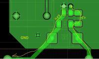
In the photo the Shape "GND" and a CLine NET "GND". Shape overlapped the CLine NET. Without clearance from it. (fig.1)
Check enabled: setup - constraint - modes - Same net spacing (fig.2)
In ConstraintManager - SameNetSpacing - Line to Shape = 0.2mm (fig.3)
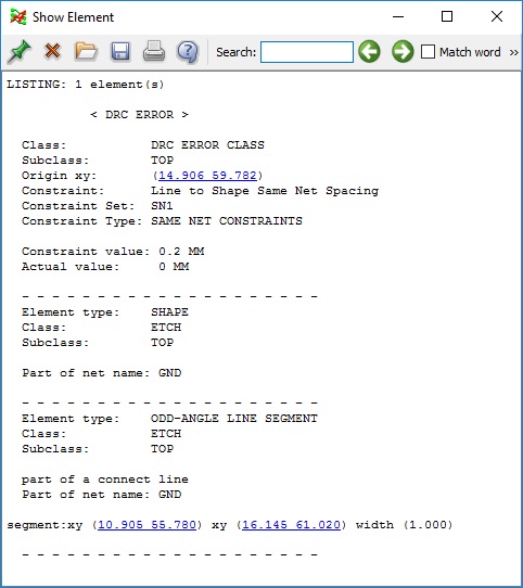
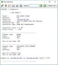
You can see DRC errors: "Line to Shape Same Net Spacing" (fig.4)
How to make an clearance of the CLine from the Shape, which belong to the same electrical circuit? As well as with the electrical circuit located to the right (+5V)
PS:
I can use Property Edit: Add "VOID_SAME_NET" for selected CLine.
But this method is an exception, for single lines.
I think there should be a global setting for this. Maybe ConstraintManager?
I need help.
Hello.
In the photo the Shape "GND" and a CLine NET "GND". Shape overlapped the CLine NET. Without clearance from it. (fig.1)
Check enabled: setup - constraint - modes - Same net spacing (fig.2)
In ConstraintManager - SameNetSpacing - Line to Shape = 0.2mm (fig.3)
You can see DRC errors: "Line to Shape Same Net Spacing" (fig.4)
How to make an clearance of the CLine from the Shape, which belong to the same electrical circuit? As well as with the electrical circuit located to the right (+5V)
PS:
I can use Property Edit: Add "VOID_SAME_NET" for selected CLine.
But this method is an exception, for single lines.
I think there should be a global setting for this. Maybe ConstraintManager?
I need help.
FIG.2
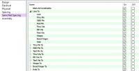
FIG.3
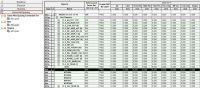
FIG.4
In the photo the Shape "GND" and a CLine NET "GND". Shape overlapped the CLine NET. Without clearance from it. (fig.1)
Check enabled: setup - constraint - modes - Same net spacing (fig.2)
In ConstraintManager - SameNetSpacing - Line to Shape = 0.2mm (fig.3)
You can see DRC errors: "Line to Shape Same Net Spacing" (fig.4)
How to make an clearance of the CLine from the Shape, which belong to the same electrical circuit? As well as with the electrical circuit located to the right (+5V)
PS:
I can use Property Edit: Add "VOID_SAME_NET" for selected CLine.
But this method is an exception, for single lines.
I think there should be a global setting for this. Maybe ConstraintManager?
I need help.
Hello.
In the photo the Shape "GND" and a CLine NET "GND". Shape overlapped the CLine NET. Without clearance from it. (fig.1)
Check enabled: setup - constraint - modes - Same net spacing (fig.2)
In ConstraintManager - SameNetSpacing - Line to Shape = 0.2mm (fig.3)
You can see DRC errors: "Line to Shape Same Net Spacing" (fig.4)
How to make an clearance of the CLine from the Shape, which belong to the same electrical circuit? As well as with the electrical circuit located to the right (+5V)
PS:
I can use Property Edit: Add "VOID_SAME_NET" for selected CLine.
But this method is an exception, for single lines.
I think there should be a global setting for this. Maybe ConstraintManager?
I need help.
FIG.2
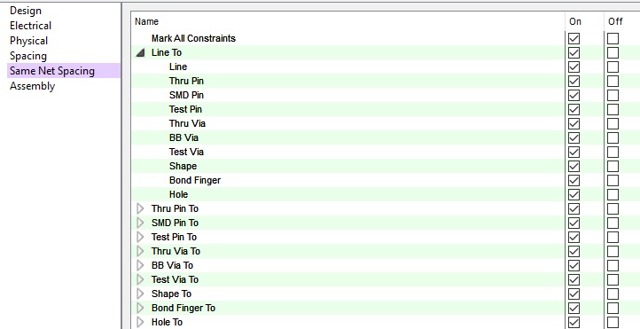
FIG.3
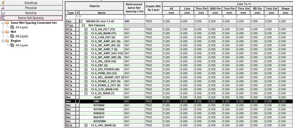
FIG.4