Continue to Site

Welcome to EDAboard.com

Welcome to our site! EDAboard.com is an international Electronics Discussion Forum focused on EDA software, circuits, schematics, books, theory, papers, asic, pld, 8051, DSP, Network, RF, Analog Design, PCB, Service Manuals... and a whole lot more! To participate you need to register. Registration is free. Click here to register now.

Different footprints for the same potentiometer. Which one to use?

Status
Not open for further replies.

venn_ng

Member level 5
Joined
Mar 26, 2017
Messages
87
Helped
1
Reputation
2
Reaction score
1
Trophy points
18
Activity points
645
Hi,

I have a question regarding the footprint of a potentiometer.

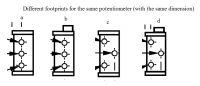
I saw few datasheets and I find that there are few possible footprints for a potentiometer even though the dimensions are the same, as shown below.


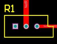
The footprint that I have on my Altium PCB layout is this


Questions
1) Why do we have different footprints for the potentiometer with the same dimenions; what's the purpose?
2) Based on the footprint that I have on my Altium PCB layout, can I say that it's the same as (b) in the first figure shown?

Thanks!
 

You are working in the wrong way, first decide which potentiometer you want to use on the pcb. Then create a symbol and the footprint and use those on the design.

And Yes, there are a lot of different footprints, But this applies to a lot of components. Never choose a footprint and then try to find a part that fits on that footprint.

I have found the potentiometer and it has the footprint (b), as shown in the first figure. Is this the same as what I have on the PCB layout shown above in the second figure?
 

Can anyone please reply to my question?
I have found the potentiometer and it has the footprint (b), as shown in the first figure. Is this the same as what I have on the PCB layout shown above in the second figure?
 

If you look at those images of pots hey are not the same.

You have both vertical and horizontal versions, straight pins and staggered pins.

The body molding of the pot is the only thing that is the same.

For this reason, you need more than 1 footprint if you are going to use them all.
 

Hi,

Yes, b is the same as the PCB layout. Or rather, yes and no - if the PCB shows the underside of the board where the soldered pins go, then yes; if the PCB shows the top, where the trimpot body will be, then no - the screw/dial will be on the other side to the PCB footprint when placed. In your mind's eye, turn the drawing 90º clockwise, then rotate the trimpot 180º on the horizontal plane and you'll see. 90º anti-clockwise will have the screw on the right side of the PCB layout but it'll be at the upper, not lower half.

It seems to be for the side screw version pot, rather than the version with the screw/dial on the top.
 
Last edited:

Status
Not open for further replies.

Part and Inventory Search

Welcome to EDABoard.com

Sponsor

Back
Top