Continue to Site

Welcome to EDAboard.com

Welcome to our site! EDAboard.com is an international Electronics Discussion Forum focused on EDA software, circuits, schematics, books, theory, papers, asic, pld, 8051, DSP, Network, RF, Analog Design, PCB, Service Manuals... and a whole lot more! To participate you need to register. Registration is free. Click here to register now.

Lock in amplifier, Phase sensitive detection, demodulation

Status
Not open for further replies.

Karolina_1

Member level 3
Joined
Mar 10, 2017
Messages
67
Helped
0
Reputation
0
Reaction score
1
Trophy points
8
Activity points
639
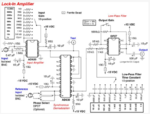
Hi, I was trying to build lock in amplifier as it was explained in Instructables with simple AD630, AD620, OP27 and 3rd order low pass filters(R1=R2=R3=10kohm C1=C2=C3=3.3microF). I generated reference and input signal from signal generator and made their phase and frequency equal. Ref and input signal are phase locked loop inside the signal generator. Reference and input signals are both 200mVpp or 70.7mVrms, f=1kHz. I adjusted both AD620 and OP27 gain to 10. AD620 working fine, i can see 700mVrms & 2Vpp f=1kHz and after demodulation Vpp=2 and Vrms becomes 0.61mVrms, f=2kHz. After some filters and OP27 at the output i see 11.1V DC. I think i was supposed to see 7V DC.(70.7mVrms*10(gain)*10(gain))I want to use this lock in amplifier as a voltmeter to measure signals in noisy environment. How output DC voltage and input signal are related? Maybe filters gain is the reason for wrong output. I took out the 100microF capacitor at the output.

More detailed explanation of project is here.
https://www.instructables.com/id/Lock-in-Amplifier/

Best regards Capffture.PNG
Thank you
 

Hi,

use a scope and show these signals in one single picture:
* INPUT
* TEST
* REFERENCE INPUT
* OUTPUT

Klaus
 

aaa.jpg

Reference and input signals are one point to the left. In other words input signal 2.04Vpp actually 0.204Vpp(204mVpp). and the relation that i found btwn input Vpp and output Vdc is 14.49. In simple words if input is 200mVpp, output is 200/14.49=13.8V DC.

thanks for reply
 

Everything as expectable:

AD630 input 2Vpp sine (0.7 Vrms)

Averaged rectified value 1 Vp *2/pi = 0.637 V
AD630 gain = 2, AD630 output 1.27 Vavg

OP27 gain = 11, Vout,dc = 13,97 V
 
Hi,

use a scope and show these signals in one single picture:
I asked for all signals in one scope picture, so that I'm able to see phase differences, because output voltage depends on phase difference.

Klaus
 

I asked for all signals in one scope picture, so that I'm able to see phase differences, because output voltage depends on phase difference.
Demodulated output waveform shows that signal and reference are perfectly in phase, achieving maximum output signal.

I'm not sure which questions are still open. The measurement almost matches the expectable output, +/- some resistor tolerances and measurement inaccuracy.
 

thank you. its very good information
 

Status
Not open for further replies.

Similar threads

Part and Inventory Search

Welcome to EDABoard.com

Sponsor

Back
Top