Continue to Site
Follow along with the video below to see how to install our site as a web app on your home screen.
Note: This feature may not be available in some browsers.
is there a depletion region in MOS when VFB < VGB < 0?
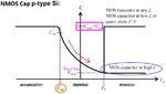
The capacitance of this space charge region is in series with the oxide capacitance, thus correspondingly reduces the total MOS capacitance, s. e.g. the explanation from **broken link removed**, where I took the **broken link removed** from.the positive charge on the gate (compared to VFB) pushes the mobile holes into the substrate. Therefore, the semiconductor is depleted of mobile carriers at the interface and a negative charge, due to the ionized acceptor ions, is left in the space charge region.

... I don't know where is the Cdep(depletion cap) ?
Please reference the attached file.
Hi mpig :Could you help me to know the depletion cap structure? like Cox.
I wish to know the two plates of Cdep.
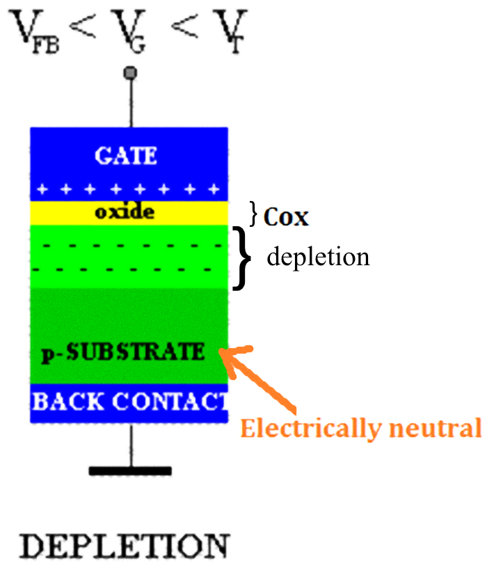
6.2.3. Depletion
As a more positive voltage than the flatband voltage is applied, a negative charge builds up in the semiconductor. Initially this charge is due to the depletion of the semiconductor starting from the oxide-semiconductor interface. The depletion layer width further increases with increasing gate voltage.
No, you are right!The distance between the gate and the bulk is tox (the width of the oxide) + Wdep (the width of the depletion region).
==>The distance is increased, so the cap value is decrease.
If I am wrong, please correct me.
Now what does depletion - here in p-type material - really mean? A positive voltage VFB < VGB < VTH at the gate attracts mobile electrons from the p-substrate in direction to the substrate-oxide interface, there filling the available Boron holes, which so constitute a fixed (immobile) negative anti-charge to the positive charge on the gate metal.
No, s. above text! Holes cannot be repelled, they are fixed, immobile (Boron) atoms in the (Silicon) lattice. VGB attracts mobile electrons from the p-substrate in direction to the substrate-oxide interface, there filling the available Boron holes ...==>Does it mean the hole repel by VGB (when VGB > VFB)?
A layer of p-type substrate by this is depleted of mobile (positive) holes, which now are replaced by immobile negatively charged Boron atoms.
Alike. A recombination means a transformation of a charged atom (an ion) into a neutral one; in this case it's the other way round: the neutral Boron atom (the hole) traps an electron and keeps it - now it has the same number of electrons as its Silicon neighbors and so holds a good equilibrium state in the lattice - however is negatively charged now: a charged atom - an ion, but a fixed & immobile charge.==>The depletion in the p-type substrate(when VGB > VFB) is formed by the recombination of electrons and holes in the Boron atoms, so this condition cause the Boron atoms is negative charge?
Hi erikl :
I know the depletion region is light green.
Could you help me to know the depletion cap structure? like Cox.
I wish to know the two plates of Cdep.
I think the Ctol = Cox serial Cdep in the depletion region that means the structure is:
one plate is gate
other plate is bulk
The distance between the gate and the bulk is tox (the width of the oxide) + Wdep (the width of the depletion region).
==>The distance is increased, so the cap value is decrease.
If I am wrong, please correct me.
Thanks.
mpig
Holes are not fixed, they are mobile!!!