venn_ng
Member level 5
Hi,
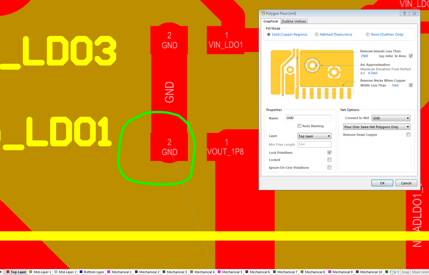
I created a GND polygon on the top layer. It's connecting all GND nets except few ones. I am including one net that's not being connected to the polygon below

Now, if I change the Net options in the Polygon Pour window to Pour over all net objects, it works.
I don't know if I can do that and if that's a problem. Thanks!
I created a GND polygon on the top layer. It's connecting all GND nets except few ones. I am including one net that's not being connected to the polygon below
Now, if I change the Net options in the Polygon Pour window to Pour over all net objects, it works.
I don't know if I can do that and if that's a problem. Thanks!