venn_ng
Member level 5
Hi,
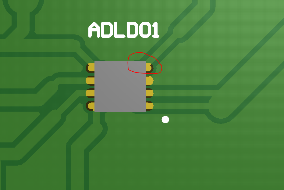
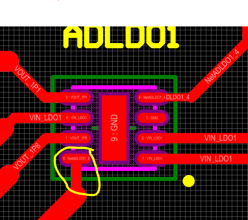
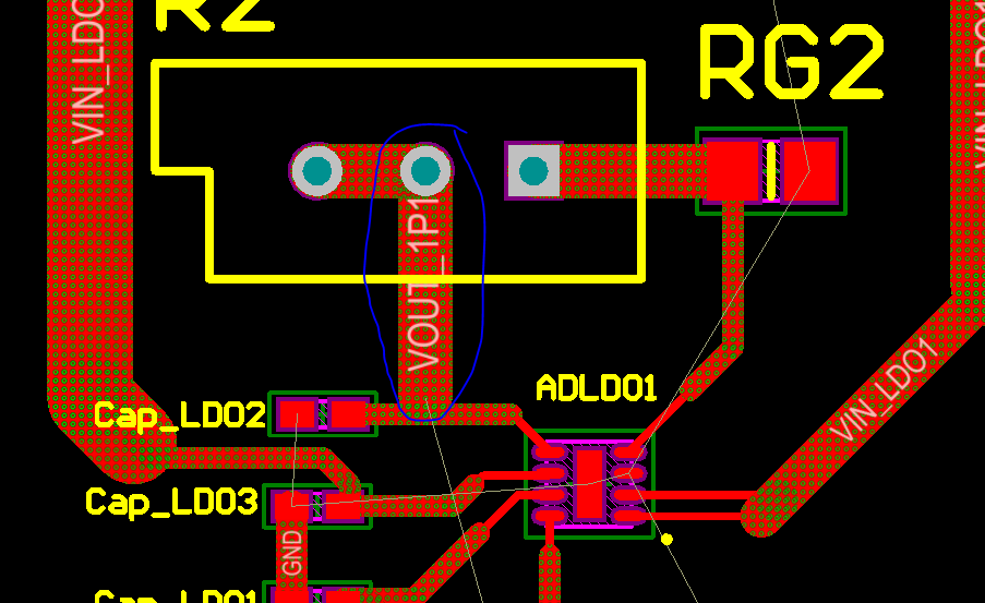
I see that the routings in a PCB don't turn by 90 degrees to avoid the hard discontinuity for the flow of electrons. My question is if that's the case is the following routing (marked in blue) not recommended? Should it be curved?
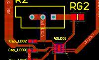
I see that the routings in a PCB don't turn by 90 degrees to avoid the hard discontinuity for the flow of electrons. My question is if that's the case is the following routing (marked in blue) not recommended? Should it be curved?
Last edited by a moderator: